


Benefits of Surface Pressure Measurement in CMP and Post CMP Processes

The Chemical Mechanical Polishing process is widely used in fabrication of semiconductor devices and has evolved from a required process to facilitate multiple layer Back End of Line (BEOL) interconnects to a process enabler in advanced front end of line (FEOL) planar and 3D integration schemes. As the number of CMP steps increase in advanced technology node devices, the number of materials and process consumables continue to evolve. This diversity of CMP processing places an increasing emphasis on control of the CMP tool configuration to facilitate a wide portfolio of process variables. It is well known that polishing pressure plays a significant role in the resulting material removal rate. Many published articles in literature have discussed mathematical modeling of the contact pressure between the polishing pad and the wafer and the corresponding correlation to experimental results.
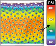
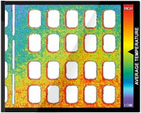
However, one of the challenging aspects of the numerical modeling approach is that the real pressure distribution at the pad wafer interface is impacted significantly by the pad surface contact area, which is a function of the porosity of the polishing pad. The below image illustrates the typical contact between the pad surface and the wafer and the corresponding variability of the pad wafer contact area occurring due to the contact profile.

Contact pressure interface between wafer and polishing pad and corresponding radial contact pressure distribution
Results such as those shown in the radial contact pressure distribution data are published in various articles [1,2] that demonstrate the importance of quantifying the real contact pressure between the polishing pad and the wafer. Many literature sources refer to the mechanism for material removal in CMP in terms of mathematical probability of the local pad surface hardness exceeding an activation level in order to generate sufficient energy for material removal.
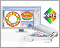
The above pressure distribution profile is captured using a static pressure measurement film that senses applied pressure by transfer of pressure sensitive capsules to a receiving film. The pressure measurement equipment provides quick static characterization of the pressure profile between contacting surfaces and provides an insight into the instantaneous load applied to the wafer by the wafer carrier system. The equipment required in this case is simply the sheet of pressure sensitive film accompanied by a purpose built densitimetric scanner that can easily connect into a standard windows based operating system using accompanying software. The software interprets the greyscale pressure map and allows zonal plot, 3D rendering and export to a spreadsheet for further data plotting.
In the above case, the real contact surface of the polishing pad is considered when evaluating the wafer backside loading provided by the CMP tool. Modern CMP tools feature multi-zone pressure control and the impact on contact pressure distribution using different combinations of zonal pressures can be quickly evaluated using this static pressure measurement approach.
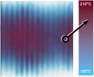
Further study of the evolution of contact pressure during pad life, the impact of different pressure ramp regimes and the progressive deformation of the polishing pad surface asperities during wafer loading or resulting from pad wear may also be achieved using a dynamic pressure mapping approach. For example, when applying initial contact pressure to the wafer, the outer retaining ring is first pressed against the pad, followed by ramp of wafer backside pressure within the air bladder zone. The changes in the pad surface asperity distribution due to the loading ramp may impact the true contact area of the pad and wafer during polishing. Depending on the number of cycles of polishing pad use, the asperities may eventually begin to viscoelastically flow into one another.

Progressive pad surface wear from wafer backside loading can be monitored by measuring contact pressure
By monitoring the contact pressure between the wafer and a typical polishing pad during various stages of pad life, the onset for excessive pad wear can be detected and the typical pad life can be predicted in a pro-active manner.
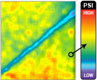
Static pressure mapping has been discussed as a method to characterize the signature contact pressure delivered by a particular CMP tool to the pad wafer interface. However, to characterize pad wear, the deformation of the pad surface deformation does not occur consistently between a new fresh pad and a worn pad due to the different regimes of viscoelastic deformation that occur after repeated loading cycles [1, 3]. Therefore, monitoring of the contact pressure over time is required to accurately study the pad wafer contact pressure dependency on pad wear.
The dynamic pressure sensor features a series of piezo-resistive elements bonded together in a repeating matrix within a thin sheet connected directly to a computer where realtime pressure monitoring is facilitated by accompanying software for a windows operating system. Similar to the static pressure mapping approach, the equipment required in dynamic pressure mapping is portable and convenient to setup. There are also other applications within the CMP tool such as monitoring the dynamic contact pressure during post CMP brush cleaning and monitoring the pad surface deformation during pad conditioning.
The PVA brush cleaning process post CMP is a particularly important application for dynamic pressure mapping in order to ensure that the probability of wafer scratching is minimized during the process. Similar to the pad wear case, it is advisable to regularly monitor the pressure map during the brush clean process to monitor the maximum local pressures.
In this white paper, static and dynamic pressure mapping during the CMP process is discussed using either pressure sensitive film or photoresistive tactile pressure skin sensors. Both sensors have convenient integration with everyday windows based personal computers and enable design of optimized wafer loading for new CMP process setup as well as facilitating important monitoring of polishing pad wear and post polish brush local pressure.