


Evaluation of Megasonic Cleaning Systems for Particle Removal Efficiency and Damaging
G. Vereecke*, F. Holsteyns, J. Veltens1, M. Lux, S. Arnauts, K. Kenis, R. Vos, P.W. Mertens, and M.M. Heyns
IMEC, Kapeldreef 75, B-3001 Heverlee, Belgium *[email protected] 1KHLeuven, Dept. REGA, B-3000 Leuven, Belgium
In future semiconductor technology generations cleaning processes will face the challenge of removing nano-particles with no damage to fragile structures and virtually no etching of the substrate. In this study we have evaluated the capabilities of a representative set of present megasonic cleaning tools to meet this challenge in process conditions where the etching of thermal silicon dioxide was lower than 0.5 Å. The tests vehicles for particle removal and damaging consisted in 34 nm SiO2 particles on hydrophilic Si wafers and in poly-on-gate lines of line-width ranging from 150 to 70 nm, respectively. No tool reached the target of high particle removal efficiency (PRE) and low damage to the 70 nm lines in the present series of tests. Lower damage could only be obtained at the cost of lower PRE, by decreasing the megasonic power. Wafer maps for PRE and damage showed patterns that were tool-specific. Only two systems out of five seemed to show a simple direct correlation between PRE and damage at wafer level, indicating that more fundamental research is needed to understand the cleaning and damaging mechanisms in megasonic systems.
INTRODUCTION
In semiconductor manufacturing, as features sizes are scaling down below 100 nm, particles with a diameter of a few tens of nanometers need to be considered as killer defects. For example with the 90nm technology node particles of a size larger than 45nm are believed to be potential killer defects for devices in chips.1 For several reasons related to substrate consumption budget, cost, and environmental impact, present cleans make use of diluted chemistries with low etching capability and need additional physical mechanisms, such as megasonic agitation, to remove contaminant particles.2 As particle size decreases, the ratio of adhesion force over cleaning force increases, thereby potentially compromising the particle removal efficiency (PRE).3 On the other hand, wafer surfaces may present fine structures with fairly high aspect ratios, such as gate electrodes or low k isolation patterns, which become vulnerable to sideward impact by physical forces.4,5 The combination of all these trends results in a collapse of the process window to the extent that cleaning of nano-particles is becoming a major challenge in production and the future use of traditional cleaning methods is questioned.
Previous studies have demonstrated that, even though cleaning of nano-particles is becoming increasingly more difficult as particle size decreases, it is actually possible to remove particles with a diameter as small as about 30 nm by megasonic cleaning.6,7 PRE was shown to depend strongly on the presence of dissolved gas in the cleaning solution, indicating that cavitation was playing an important role in the cleaning mechanism.8,9 The decrease in PRE at smaller particle size was associated with a decrease in cleaning uniformity.
In this work various megasonic cleaning systems were evaluated for removal efficiency of nano-particles, cleaning uniformity, and damaging of fragile structures, providing a snapshot of the capabilities of present tools to respond to the new challenges. Additionally comparison of wafer maps for PRE and damaging was used to better characterize the relationships between PRE and damaging.
MATERIALS AND METHODS
The cleaning tests were performed in various systems (A, C to F) differing by their configuration (batch or single-wafer, position of transducers, carrier), solution flow (recirculation or single-pass), transducer operation (continuous or multiplexed), and wafer size (200 or 300 mm) (Table 1). Transducer frequencies ranged from 0.7 to 1 MHz. The effect of dissolved gases was studied by comparing results obtained with degassed and aerated DIW. PRE was determined with hydrophilic 200 or 300 mm Si wafers contaminated with SiO2 particles of 34nm diameter purchased as slurry (Clariant Elexsol). Wafers were contaminated using an immersion based controlled contamination (CC) procedure and used within a few hours after preparation.10 Particles numbers were determined using light scattering on a KLA Tencor SP1TBI using the haze channel.10,11 Particle removal efficiencies (PRE) were calculated from measured particle counts after CC and after clean, taking the initial count pre-CC into account.
Table 1. Overview of tested megasonic cleaning tools
| Tool | Version | Type | Flow | Transducer Operation | Wafer size (mm) | Carrier |
| A | α-design | Batch | Single-Pass | Continuous | 300 | No |
| C | Demo | Batch | Recirc. | Multiplexed | 200 | Low-mass |
| D | Commercial | Batch | Recirc. | Multiplexed | 200 | No1 |
| E | Commercial | Batch | Recirc. | Continuous | 200 | Low-mass |
| F | α-tool | SW2 | Single-pass | Continuous | 200 | Edge Grip |
The test vehicle for damaging consisted in 200 mm wafers with poly-on-gate lines that were inspected by laser-light scattering (KLA-Tencor AIT) and SEM (Philips XL810). The lines were 8 mm long and about 170 nm tall, with widths and aspect ratio ranging from about 150 to 70 nm and about 1.1 to 2.5, respectively (Fig. 1). The lines were printed in groups of nine, differing by line-width and spacing. External lines in groups of narrow spacing were printing thinner as a result of so-called proximity effects during photolithographic exposure (see Fig. 1, left). Finally the pressure distribution at the surface of wafers during cleaning was determined with wafers covered with a pressure indicative sensor film (Pressurex Micro, from Sensor Products Inc.).12
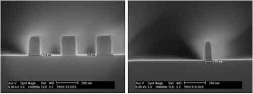
Fig. 1. SEM view of poly-gate lines with line-width of about 140 nm (left) and 70 nm (right), respectively.
RESULTS AND DISCUSSION
With all megasonic-cleaning tools damaging of poly lines showed up in SEM inspection as the removal or bending of small pieces of line with a length of about 1 to 2 µm (Fig. 2). The localized character of damage suggests that cavitation was probably the cause. Full wafer inspection with a KLA-Tencor AIT could only detect the removed pieces of line but allowed to determine defects statistics and the spatial distribution of defects on wafers.

Fig. 2. Representative SEM views of 70 nm poly-gate lines damaged by megasonic cleaning, showing removed (left) and bended (right) pieces of line.

Fig. 3. Poly-gate lines damage frequency distribution as a function of line-width and aspect ratio (tool E, APM 1:1:80 at 30°C, 5 min, 100 % power).
Figure 3 shows a typical frequency distribution for damage of these poly lines as a function of line-width and aspect ratio. Calculations took into account the area covered by groups of lines and the thinning of external lines with narrow spacing. Line-width bins were defined with a range of about ±5 nm from 70 to 110 nm and a range of about ±10 nm from 120 to 150 nm. Comparable results were obtained when taking the length of lines into account instead of the area. The distribution is characterized by a strong increase in damage frequency for line-widths below 100 nm. This observation is valid for all tools and process conditions tested in this study. It indicates that present megasonic cleaning tools will suffer a dramatic reduction in process window with new technology generations.
In future generations the process window will be defined by the achievement of high removal efficiency for nano-particles with no damage to fragile structures and virtually no etching of the substrate. In Fig. 4 the density of megasonic defects per wafer for 70 nm poly lines is compared to the PRE for 34 nm SiO2 particles under process conditions where etching of thermal oxide was less than 0.5Å in most cases. In most conditions only one poly-gate line wafer was used per test. Reproducibility was checked by performing a few tests with two wafers, giving a range of variation typically of about 10 % for the total number of defects per wafer. Figure 4 shows three groups of data points, labeled I to III. Group I corresponds to cleans performed at high power in degassed solutions (< 0.3 ppm O2, single-pass). PRE was close to zero while damage was relatively high. Group II corresponds to cleans performed at high power in aerated solutions under different process conditions (chemistry, concentration, temperature). Gas dissolution resulted in significantly higher PRE but damage levels remained relatively high, increasing even in case of tool F. Finally group III gives results from tools A, C, and F where megasonic power was decreased for a given set of process parameters with aerated solution. The presence of dissolved gas in the cleaning solution as a necessary condition to remove nano-particles indicates that the cleaning mechanism was not due to acoustic streaming (Eckart and Schlichting streaming) or vapor cavitation, but rather to gas cavitation phenomena (micro-streaming, bubble implosion).8,13,14 Damaging with degassed solutions probably indicates that vapor cavitation occurred under these conditions. Only decreasing the power proved to be efficient in decreasing the number of megasonic defects, albeit at the cost of a lower PRE (group III). Apparently, from this series of tests, no tool was able to reach the target of high PRE with no damage.

Fig. 4. Damage to 70 nm poly-gate lines as a function of PRE for 34 nm SiO2 particles for tools A to F under various process conditions (see text). The asterisk (*) points to data points where etching of thermal oxide was higher than 0.5Å.
Figure 4 shows that PRE and damaging are directly correlated to megasonic power. In this line it is generally believed that PRE non-uniformity at wafer level is caused by a non-uniform acoustic pressure distribution, with lower PRE areas corresponding to lower pressures. However a close look at wafer maps obtained in this study for PRE and damaging showed that there was usually no simple correlation between PRE, damaging, and power at wafer level. This will be illustrated in the case of tools C, E, and F.
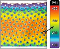
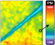
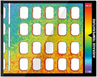
Wafer maps for PRE and damaging for tools C, E, and F are given in Fig. 5. In tool C and E the array of transducers was firing the wafers from bottom up. Patterns obtained in different process conditions were similar, differing mainly by the level of PRE or damage. Both types of maps show patterns that were tool-specific. The patterns for tool C were characterized by vertical stripes, those of tool E by higher PRE and damage along the vertical diameter, while tool F presented circular patterns corresponding to the spinning motion of the wafer during cleaning.
Although wafer maps for PRE and damaging showed striking similarities, there seemed to be a direct correlation between PRE and damaging at wafer level only in the case of tools A and E. Higher damage was observed in areas of higher PRE, as shown for tool E in Fig. 5. With tool C, the opposite was observed: stripes with higher PRE presented a lower damage and vice versa. The pressure distribution across the wafer surface was determined with pressure sensitive films, revealing stripes of higher pressure above the center of the elements of the transducer array (Fig. 6). Thus higher pressure corresponded to higher damage but lower PRE. Tool D also had multiplexed transducers, but mounted in arrays in the sidewalls of the megasonic tank, while the wafer was moved up and down during cleaning. In this case no stripe pattern was observed on the wafer maps that presented no clear correlation between PRE and damaging. Finally with tool F the highest damage was observed in an outer ring of intermediate PRE (85-95 %), while other rings of higher (95-100 %) or lower (50-85 %) PRE presented a lower damage.


Fig. 5. Wafer maps for PRE (top, 34 nm SiO2 particles) and megasonic damage (bottom, 70 nm poly-on-gate lines, NI = not inspected) for tools C, E, and F. Cleaning conditions: aerated diluted APM solutions at 20-30 °C, with an average PRE in the range of 70-90 %.

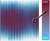
Fig. 6. Wafer map of megasonic pressure distribution for tool C. Darker areas correspond to higher pressure.
CONCLUSIONS
We have evaluated the capabilities of a representative set of present megasonic cleaning tools to remove nano-particles with low damage in process conditions where the etching of thermal silicon dioxide satisfied specifications for the 70 nm technology node. The tests vehicles for particle removal and damaging consisted in 34 nm SiO2 particles on hydrophilic Si wafers and in poly-on-gate lines of line-width ranging from 150 to 70 nm (aspect ratio 1.1 to 2.5), respectively.
All tools were capable of achieving high particle removal efficiencies (PRE) of about 80 % or higher for the nano-particle challenge. Damaging by megasonic was low for lines wider than 100 nm but started to increase dramatically for smaller line-widths. Among the parameters tested megasonic power had the most significant influence on damage. Decreasing megasonic power allowed to decrease megasonic damage to 70 nm lines, albeit at the cost of a lower PRE. As a consequence no tool reached the target of high PRE and low damage in the present series of tests.
PRE was limited by cleaning non-uniformity at wafer level, which showed toolspecific patterns. Wafer maps for damaging also showed tool-specific patterns. However in three systems out of five there was no simple direct correlation between PRE and damage at wafer level, indicating that more fundamental research is needed to understand the cleaning and damaging mechanisms in megasonic systems.
ACKNOWLEDGEMENTS
The authors thank S Beckx and P. Jaenen for their help in preparing the damaging test wafers, M. Lismont for setting up the recipe on the KLA-Tencor AIT, and G. Doumen for technical assistance with the megasonic systems.
REFERENCES- The International Technology Roadmap for Semiconductors (Semiconductor Industry Association, San Jose, CA, 2001) p.16
- H. Kawahara, in: Ultraclean Surface Processing of Silicon Wafers (T. Hattori, ed.), Springer (1998) pp. 451-461
- M. Olim: J. Electrochem. Soc., 144, 3657 (1997)
- A. Tomozawa, H. Kinoshita, Y. Sakata, A. Ohnishi, Y Harada, and N. Hiraoka, ECS 5th Int. Symp. Cleaning Technol. Semicond. Device Manuf., September, 1997, Paris, France (Electrochem. Soc. Proc., PV 97-35, 79 (1998))
- P. Mertens and E. Parton, Solid State Technology, 45, 51 (2002)
- J. Lauerhaas, Y. Wu, K. Xu, G. Vereecke, R. Vos, K. Kenis, P.W. Mertens, T. Nicolosi, and M.M. Heyns, ECS 7th Int. Symp. Cleaning Technol. Semicond. Device Manuf., September 2-7, 2001, San Francisco, CA (Electrochem. Soc. Proc., PV 2001- 26, 147 (2002))
- P.W. Mertens, J. Lauerhaas, F. Holsteyns, R. Vos, M.O. Schmidt, G. Vereecke, Kaidong Xu, W. Fyen, M. Baeyens, S. Arnauts, K. Kenis, and M.M. Heyns, 2002 Symp. on VLSI Technology, Honolulu, HI, USA, June 11-13, 2002 (IEEE Electron Device Soc. & Japn. Soc. Appl. Phys.)
- F. Holsteyns, G. Vereecke, V. Coenen, R. Vos, and P.W. Mertens, Forum Acusticum 2002, Sevilla, Spain, September 16-20 (2002)
- G. Vereecke, R. Vos, F. Holsteyns, M.O. Schmidt, M. Baeyens, S. Gomme, J. Snow, V. Coenen, P.W. Mertens, and M.M. Heyns, Solid State Phenom., 92, 143 (2003)
- K. Xu, R. Vos, G. Vereecke, M. Lux, W. Fyen, F. Holsteyns, K. Kenis, P.W. Mertens, M.M. Heyns and C. Vinckier, Solid State Phenomena, 92, 161 (2003)
- S.H. Yoo, B.Y.H. Liu, J. Sun, N. Narayanswami, and G. Thomes, Solid State Phenomena, 76-77, 259 (2001)
- G. Vereecke, F. Holsteyns, J. Veltens, R. Vos, and P.W. Mertens, Ultrasonics Int. Conf., UI03, Granada, Spain, July 1-3 (2003)
- F. Holsteyns, A. Riskin, G. Vereecke, and P.W. Mertens, these proceedings
- F.R. Young: Cavitation (Imperial College Press, London, 1999)
