


Redesign of the SNS Modulator H-Bridge for Utilization of Press-Pack IGBTs
Mark A. Kemp and Craig Burkhart
Stanford Linear Accelerator Center
2575 Sand Hill Road
Menlo Park, CA 94025, USA
David E. Anderson
Oak Ridge National Laboratory
Oak Ridge, TN 37831, USA
Abstract
The power conversion group at SLAC is currently redesigning the H-bridge switch plates of the High Voltage Converter Modulators at the Spallation Neutron Source. This integral part to the modulator operation has been indentified as a source of several modulator faults and potentially limits reliability with pulse width modulation operation. This paper is a presentation of the design and implementation of a redesigned switch plate based upon press-pack IGBTs.
Index Terms Insulated gate bipolar transistors, power conversion, power electronics, power modulation, power semiconductor devices, pulse circuits, pulse power systems.
1. Introduction
The High Voltage Converter Modulators (HVCMs) at the Spallation Neutron Source (SNS) have operated for well in excess of 200,000 hours. There are several configurations of HVCMs at SNS with output voltages in the range of 75-125 kV, peak powers of up to 11 MW, and average powers up to 1 MW. These modulators were developed at Los Alamos National Laboratory and have been configured for application at SLAC and KAERI in addition to SNS [1-3].
There are several advantages to this topology such as a relatively high efficiency of >93%, automatic fault ridethrough capability, and reduced switching losses due to zerovoltage turn-on. A simplified system diagram is shown in Figure 1 and a detailed overview is found in [1]. Unfortunately, there have been an unexpectedly large number of failures of the HVCMs at SNS. While some improvements such as the implementation of a dynamic fault detection chassis have demonstrated improved reliability, there is still room for improvement [4,5]. The modulator was originally designed to operate with pulse width modulation (PWM) to achieve a well-regulated output pulse. This has been demonstrated successfully at low pulse repetition rates, but failures have occurred at higher average powers [1].
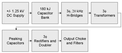
Figure 1. Simplified system diagram of the SNS HVCM.
One performance bottleneck of the HVCM is the H-Bridge switch plate. Since mid 2006 to early 2008 it has caused twenty HVCM failures including five fire events. In addition, one reason for the inability to successfully operate with PWM may be due to insufficient headroom for the associated increased switching losses. At SLAC, we have undertaken a project to upgrade the switch plate design. A significant portion of this upgrade has been to incorporate press-pack IGBTs [6].
Press-pack packages offer several advantages over flat-pack packages. First, the devices can be cooled on two sides rather than only on a single side. This offers a better avenue for heat removal. Second, press-pack IGBTs have demonstrated increased reliability in pulsed-power applications. Third, the press-pack devices do not fragment and disassemble during failure events. This reduces collateral damage to other modulator components during a failure event [7]. Finally, because the anti-parallel diode and IGBT are in separate packages, a failure in a diode does not necessarily require replacement of a more costly IGBT.
For the redesign, IGBTs have been chosen which have a higher voltage margin compared to the existing devices (3.3 kV vs. 4.5 kV). Also, MOVs were included in parallel with he IGBTs to clamp large voltage transients. These changes along with increased cooling capacity will help improve switch plate reliability during PWM operation.
This paper is a presentation of some aspects of the design process for replacing the flat-pack IGBT switch plate with a switch plate that incorporates press-pack devices. Detailed analysis of key issues is given. Specifically detailed are how the mechanical layout was made to reduce the potential for arcing between buses, the calculation of the stray inductances of the new design, and the verification of proper clamping force and pressure on the devices. This design review serves to benefit engineers who may partake in similar redesigns to incorporate press-pack devices.
2. Press-Pack Design
2.1. Mechanical Layout
The circuit schematic for the SNS H-bridge switch plate is shown in Figure 2. Detailed analysis of the switching waveforms can be found in [1]. There are several electrical differences between the existing flat-pack switch plate and the press-pack design. First, the IGBT and diode reside in different packages and each are individually cooled. Second, the new design includes a MOV to clamp voltage transients. Finally, the stray inductances of the two designs are different. A detailed analysis of these inductance values and their effect is presented in section 3.
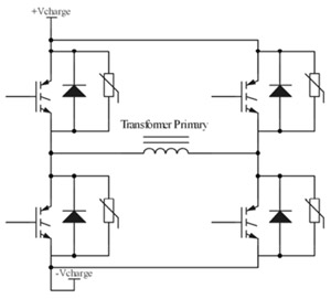
Figure. 2. Schematic of the H-bridge switch plate. Additionally, 60 µF is across the voltage buses on each switch plate. The existing flat-pack version does not include parallel MOVs.
One constraint for the new switch plate is that it be easily integrated into the existing HVCM systems. Complete replacement of the switch plate would add unnecessary expense. A rendering of the press-pack switch plate is shown in Figure 3. The snubber capacitors (Figure 3, note 6) and DC bus connections (Figure 3, note 4) are identical to the existing switch plate. Current flows from the DC bus, through the bottom heat sink, through the semiconductor devices, through a thin, copper bus, then down to the transformer primary. High current connections are made utilizing Bal-Seal balcontact springs. Commercial water cooled heat sinks were chosen for both the top and bottom of the semiconductors. The clamps were designed and built at SLAC. Details on the clamps are given in section 2.2.
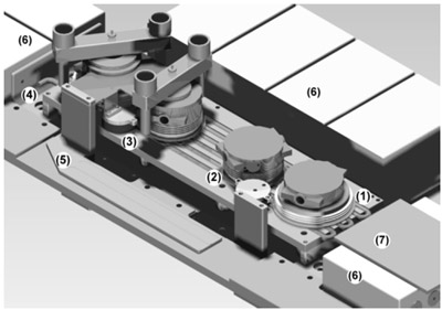
Figure 3. Rendering of the press-pack switch plate. (1) IGBT, (2) diode, (3) MOV, (4) DC bus, (5) connection to transformer primary, (6) snubber capacitors, (7) gate drive mounting location. Shown is the positive side of the Hbridge. The negative portion is on the opposite side.
There have been several failures in the SNS HVCMs directly attributed to the high potential across close conductors in the existing switch plate. A result of one failure is shown in Figure 4. If the two buses short, the 180 kJ capacitor bank discharges through the arc. Different potential conductors were kept far apart in the new design. For the parts that were changed, creep distances are greater than 1” and air-gap distances are greater than 0.5”. In particular, movable connections such as the water cooling pipes can now not be unintentionally bent to short two connections. The water cooling plate under the devices is at the same potential as the DC bus and the nearby capacitor connections. No additional dielectric spacers are necessary to ensure parts do not short.

Figure 4. Photograph of a flat-pack switch plate failure at SNS due to arcing between two close conductors.
In the existing switch plate, the IGBT gate drivers are mounted directly above the IGBTs. While offering a lowinductance lead to the IGBTs, the drivers are difficult to access. It is difficult for technicians to lean inside the modulator to adjust the gate drivers or make connections. In the press-pack design, the drivers are mounted over the side snubber capacitors (Figure 3, note 7). The lead distance is still short, but the gate drivers are in a more accessible location.
2.2. Clamp Design
One potential drawback of utilizing press-pack devices is the relative difficulty in mounting. Determined by the specific package, there must be an evenly applied force on the disk faces anywhere from 5 kN to over 45 kN (1,100 lbf to 10,100 lbf). Ideally, the force is applied to the center of the device and a force spreader is utilized to ensure an even pressure over the disk surface. Uneven pressure can lead to hot-spots and therefore derated cooling performance [8].
The clamping scheme designed for the switch plate is illustrated in Figure 5. On the top, a steel bar compresses a Belleville spring set against a steel plate. The springs were chosen such that the force required for the press-pack device was within their working range. A given applied force results in a known spring deflection. A calibration pin (figure 5, note c) with a movable disk of precise thickness was inserted between the top clamping bar (figure 5, note b) and the steel plate (figure 5, note e). When the springs deflect a certain distance, the compressed disk will no longer move. This signifies to the assembler to stop tightening the bolts.
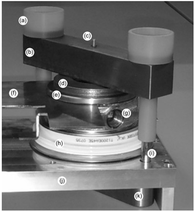
Figure 5. Photograph of a SLAC designed press-pack clamp. (a) G10 electrical isolator, (b) steel clamp, (c) force calibration pin, (d) Belleville springs, (e) steel plate, (f) copper bus, (g) commercial water-cooled heat sink, (h) IGBT, (i) 3/8 grade-8 bolt, (j) commercial heat sink (aluminum blank shown in photograph), (k) steel clamp.
A copper bus (figure 5, note f) electrically connects the IGBT to the anti-parallel diode. The flexibility of copper allows for mechanical compliance between the two packages which may not have identical thicknesses. The thickness of the copper was chosen to be greater than the electrical skin depth, yet thin enough to not impart a force of greater than 100 lbf when the press-pack devices had a diffference of thickness up to 1 mm.
The clamping bolts pass through the bottom heat sink and thread into a steel bar. While this does not ideally apply a force to the center of the device, deflection will be minimal due to the thickness and strength of the clamping bar. If the bottom clamp were not thick and stiff, the heat sink would pull away from the press-pack face at the center of the device.
Spatially homogenous pressure with acurate total force is critical to device performance. A test was conducted to confirm the clamp performance was as designed. To do so, Fuji Prescale film was placed on each of the faces of the press-pack devices [9]. This film produces a color with intensity corresponding to the applied pressure. Both the total force (spatially-integrated pressure) and uniformity of applied pressure can be measured.
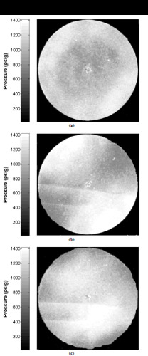
Figure 6. Measured pressure
distribution on the (a) top of
the IGBT face, (b) bottom of the
IGBT face with first clamping
scheme, and (c) bottom of the
IGBT face with shim inserted
above bottom clamping bar.
Results from one set of tests are shown in Figure 6. The film was placed above and below an IGBT, and the clamps were tightened to the designed pressure. The clamps were untightened, the film was removed and digitized with a scanner, and intensities were mapped to pressure using Matlab [10].
Figure 6a shows the pressure profile along the top of the IGBT. Because this surface is clamped from the center and a large-thickness force spreader is used, the pressure apears fairly symettric. Figure 6b shows the pressure profile on the bottom of the IGBT. Because the force is not applied from the center, intense areas appear at the sides of the IGBT where the bottom clamping bar contacts the heat sink. Some dies within the press-pack package may experience insufficient cooling with this scheme.
A ~2 in2, 8 mil. thick shim was placed between the bottom clamping bar and the heat sink. The shim was aligned axially with the IGBT. The new pressure profile is shown in Figure 6c. This alteration resulted in a more even pressure distribution. This film also indicated areas of uneven surface on the bottom heat sink. These are shown as two horizontal bright lines on the left side of both Figure 6b and 6c.
Even if the pressure distribution appears even, there is a potential that the overall force on the device is not appropriate. The pressure distributions of all three plots were spatially integrated. The resulting forces were all within the designed tolerances. In addition, the calculated forces for all the profiles in Figure 6 were within 5% of each other. Even though the pressure profile changed, the total force was the same.
3. Finite-element Inductance Calculation
The stray inductance in the switch plate is important for two primary reasons. During IGBT turn-off, there is a large di/dt. Stray inductance between the snubber capacitors and the point that the IGBTs connect to the transformer primary bus will therefore induce voltage spikes across the semiconductor devices. If the voltage spikes are excessive, device failure may result. Partially mitigating this failure mode are parallel MOVs which clamp transients above a certain level. However, to ensure low power dissipation in the MOV, designs should still minimize excessive inductance.
Stray inductances are additionally important with regard to the failure mode of shoot-through. During shoot-through, IGBTs on one side of the H-bridge (for whatever reason) conduct simultaneously. This low impedance path results in a large spike in current and eventually leads to device failure. One issue is that even if the fault is quickly detected, the current magnitude and/or di/dt may be too large to have an IGBT that can be controlled by the gate. Additional inductance in the shoot-through path results in smaller peak currents and di/dt during failure and therefore increases the probability that a detected fault can be suppressed. In other words, inductance should be minimized in the proper conduction path, but maximized in the shoot-through path.
While estimations of inductance can be made using simple equations, complex geometries such as the switch plate become increasingly difficult to calculate accurately. Finite element (FE) simulations using FastHenry were performed on both the original switch plate and the press-pack switch plate [11]. The primary goal of performing these simulations was to estimate the relative electrical effects of using a press-pack based switch plate. While there may be factors which add to the absolute simulation error (e.g. internal semiconductor device inductance, imprecise switch plate geometry rendering, etc.), simulations provide a straightforward method for estimating the relative effect of geometry changes on electrical performance.
The geometry used for simulation of the press-pack switch plate is shown in Figure 7. This encompasses the major parts of the system. For simplicity, only the IGBT was modeled; the diode and MOV were omitted. Shown are both the normal and shoot-through conduction paths.
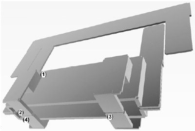
Figure 7. Geometry utilized for FE simulations. One shoot through path is defined as current flowing from (1) to (2) to (4) to the IGBT on other side of the H-bridge. A normal conduction path is from (1) to (2) through the primary to (3) to IGBT on the other side of the H-bridge.
The most significant results from these simulations are shown in Table I. Shown are the effective inductances during normal and shoot-through conditions. The press-pack design has a 40% higher inductance during normal conduction. However, during a shoot-through condition, the path inductance is nearly twice that of the original design. This may aid in suppression of device failure during a detected shoot-through condition.
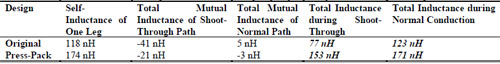
Table 1. Inductances found through FE simulation of the existing and press-pack switch plates. Paths are as defined in Figure 7.
A circuit simulation of the IGBT current during a shootthrough condition is shown in Figure 8. Simulations for the two designs are identical except for the inductance matrices utilized. The di/dt for the original and press-pack design are 47 kA/µs and 15 kA/µs respectively. The ~3x lower value increases the likelihood of the ability to turn off a detected fault. Although lower, the large fault di/dt may necessitate inclusion of a common-mode choke in future designs.
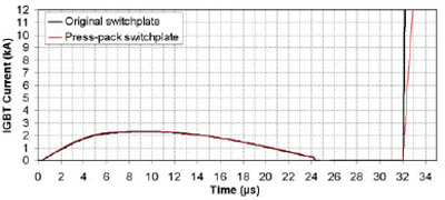
Figure 8. Circuit simulation of the IGBT collector current during a shootthrough fault condition. A fault is induced at 32 µs. Parameters are identical for both simulations except for the stray inductance matrices utilized. Inductance values were calculated using FE simulations.
The difference in inductance between the shoot-through and normal operation is due to the relative placement of the conducting IGBTs. During shoot-through, the IGBTs are approximately in a low-inductance, parallel-plate configuration. The enclosed flux is very low. During conduction, the spacing between IGBTs is large because they are at opposite ends of the switch plate.
4. Experiment
The large number of HVCMs at SNS and the relative difficulty of retuning and adjusting components necessitate a new switch plate which does not have significantly different switching waveforms than the existing switch plate. A low average power, full peak power, single-phase test stand was build at SLAC. This simulates the operating conditions of the switch plate and allows a direct comparison between the press-pack switch plate to the existing design. In addition, fault conditions can be induced in a controlled environment.
Both versions of the switch plate were separately installed in the test stand and the switching waveforms were measured. The MOV was omitted during these tests such that a direct comparison could be made. As shown in Figure 9, the IGBT collector currents and the collector-emitter voltages are approximately equal for both versions. This gives confidence of minimal impact on the modulator electrical characteristics when the existing switch plate is replaced by the press-pack switch plate.
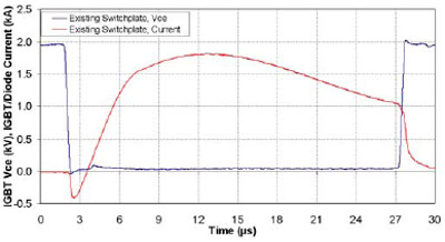
Figure 9. Measured IGBT collector-emitter voltage and IGBT/diode current for both the existing and press-pack switch plates.
With this test setup, one side effect of stay inductance can be evaluated. Inductance between the snubber capacitors and the IGBTs will induce a voltage spike during high di/dt events. This is most evident during IGBT turn-off. Shown in Figure 10, the collector-emitter voltage has a slight overshoot. Both traces are approximately equal. Therefore, it is not expected that the stray inductances during normal conduction are significantly different.
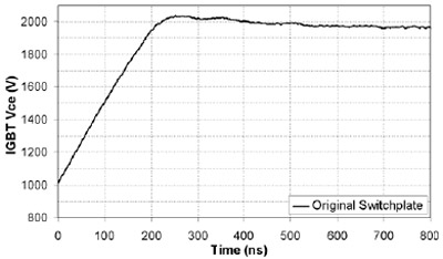
Figure 10. Measured IGBT collector-emitter voltage during turn-off for the existing and press-pack switch plates.
5. Summary
In this paper we have detailed some of the design steps undertaken to convert a flat-pack IGBT based H-bridge switch plate to one utilizing press-pack IGBTs. The mechanical layout was overviewed with specific details on the clamping mechanism. Uniform pressure was confirmed by use of pressure-sensitive film.
To evaluate the changes in stray inductance, FE simulations were used. It was found that the inductance changes in the normal conduction path were not significant, but were large in the shoot-through path. This has the impact of increasing the likelihood that a detected fault can be successfully suppressed. The switching characteristics of both switch plates were compared experimentally and were found to be nearly identical. Specifically, the additional inductance due to the press-pack design did not cause a large overshoot in the IGBT turn-off collector-emitter voltage.
Utilization of flat-pack IGBT packages is widespread and the packaging is successful in many implementations. The press-pack packaging has advantages for our particular application and a redesign of the switch plate was necessary. This note serves as a brief overview of the design steps we undertook. Future work includes full average power testing to ensure the heat sinking scheme is adequate. In addition, fault testing such as inducing a shoot-through condition will be undertaken. This work complements additional ongoing work on an advanced IGBT gate drive system [6].
Acknowledgement
Work supported by the U.S. Department of Energy under contract DE-AC05-00OR22725. SLAC-PUB-13409
REFERENCES
- W.A. Reass, D.M. Baca, R.F. Gribble, D.E. Anderson, J.S. Przybyla, R. Richardson, J.C. Clare, M.J. Bland, P.W. Wheeler, High-frequency multimegawatt polyphase resonant power conditioning, IEEE Trans. Plasma Sci., vol. 33, no. 4, pp. 1210-1219, 2005.
- W.A. Reass, R.F. Gribble, and J. McCarthy, Polyphase resonant converter-modulators for the KAERI proton engineering frontier project accelerator klystron RF amplifier system, presented at the 28th IEEE Power Modulator Conference, May 2008.
- W.A. Reass, C. Burkhart, C. Adolphsen, T. Beukers, R. Cassel, A. de lira, C. Pappas, M. Nguyen, R. Swent, D.E. Anderson, Converter-modulator design and operations for the ILC L-band test stand, Proc. Particle Accelerator Conference, 2007.
- J.J. Mize, D.E. Anderson, J. Hicks, M. Wezensky, Dynamic fault detection chassis for the 1 MW high voltage converter modulator system at the Spallation Neutron Source, Proc. Particle Accelerator Conference, 2007.
- D.E. Anderson, J. Hicks, M. Wezensky, D. Baca, W. Reass, Operational performance of the Spallation Neutron Source high voltage converter modulator and system enhancements, Power Modulator Symposium, 2006.
- M.A. Kemp, C. Burkhart, M.N. Nguyen, and D.E. Anderson, Next generation IGBT switch plate development for the SNS high voltage converter modulator, presented at the XXIV Linear Accelerator Conference, 2008.
- F. Wakeman, W. Findlay, G. Li, Press-pack IGBTs, semiconductor switches for pulse power, in proc. IEEE Pulsed Power Plasma Science 2001, p.1051.
- B. Backlund and T. Schweizer, Recommendations regarding mechanical clamping of Press Pack High Power Semiconductors, ABB Application Note, No. 5SYA2036-01, Nov. 2002.
- Fuji Prescale Film, Fujifilm NDT, Hanover Park, IL.
- Matlab, The Mathworks, Inc., version 7.4.0, Natick, MA.
- M. Kamon, M.J. Tsuk, and J.K. White, FASTHENRY: a multipoleaccelerated 3-D inductance extraction program, IEEE Trans. Microwave Theory and Techniques, vol. 42, no. 9, pp. 1750-1758, 1994.
