G Byrne, E Ahearne, and P Timoney*
Advanced Manufacturing Science Research Centre, University College Dublin, Dublin,
Ireland
The manuscript was received on 1 June 2010 and was accepted after revision for publication on 17 August 2010.
DOl: 10.1177/09544054JEM2187
Abstract:
In the semiconductor industry, chemical mechanical polishing (CMP) is utilized to planarize the surface of silicon wafers following the lithography and deposition steps, preparing the surface for subsequent layers of interconnects. Stringent local and global planarity tolerances are imposed by the feature size decreases and wafer size increases dictated by Moore’s law. The introduction of fragile, porous, oxide materials for their low dielectric constant also increases the fragility of the wafers being processed. An issue that has received significant attention in the literature is the relationship between the pressure distributed on the backside of the wafer and the resulting interfacial pressure between the wafer and the polishing pad. The Preston relationship for polishing of glass asserted proportionality between the applied pressure and the relative velocity to the resulting material removal rate. However, the pressure distribution between the pad and the wafer is not so well understood and therefore requires a detailed investigation.
This paper presents results of a finite element model of CMP incorporating realistic boundary conditions for the wafer carrier and platen assemblies. The model predictions of interfacial contact pressure are validated by unique measurements of the contact pressure between the wafer and the pad using a static pressure measurement film and accompanying analysis software. The results demonstrate a close correlation between the model’s prediction and the measured values.
Keywords:
wafer contact pressure, chemical mechanical polishing, finite element model measurement
1 INTRODUCTION
Integrated circuitry is fabricated on silicon wafers using a cycle of rnicrofabrication processes. The outline process steps are:
(a) deposit an oxide material on the surface of the wafer;
(b) create a preselected pattern of holes or trenches on the surface of the oxide;
(c) deposit copper on the surface to fill these holes;
(d) utilize chemical mechanical polishing (CMP) to smooth out the topography and prepare the surface for the next metallization layer.
The CMP process currently achieves a high degree of planarity on both local (i.e. within one device area) and global scales (across the entire wafer surface).
*Corresponding author: Advanced Manufacturing Science Research Centre, University College Dublin, Dublin, Ireland. email: [email protected]
The CMP process currently achieves a high degree of planarity on both local (i.e. within one device area) and global scales (across the entire wafer surface). The semiconductor industry continues to evolve to a smaller feature size of transistor every 24 months in accordance with Moore’s law. This evolution allows decreases in device size and thus permits increasing processing power per chip. However, the number of holes or trenches required of the lithographic patterning process is increased and this has the effect that the CMP process must perform smoothing of increasingly extreme topographical variations. The anticipated introduction of 450 mm wafers also creates a need for further optimization of the wafer pressure distribution in order to control and optimize polishing rates over larger areas.
2 ROLE OF CONTACT PRESSURE IN CMP
There has been much discussion in the literature on the importance of interfacial pressure between the pad and the wafer as a control parameter for CMP. Preston [1] proposed that the material removal rate in polishing is equal to the product of applied pressure, the relative velocity between the pad and wafer, and a constant of proportionality. Tseng et aL [2] proposed a modified relationship where removal rate was defined as the product of a new weighting proportionality constant, pressure raised to the power of 5/ 6 and velocity to the power of 1/2. Numerous efforts have been made to model the CMP process on many different length scales, from highly localized pad asperity scale [3, 4] to the full wafer scale [5]. Many efforts have also been made to optimize the load application mechanism, the wafer carrier, based on models prescribing the optimum loading on the backside of the wafer. Fu and Chandra [6] developed an analytical model that highlighted the difference between wafer loading pressure and the resulting interfacial pad wafer pressure. Weber et al. [7] developed a wafer carrier with annular individually controllable piezo-stack actuators with the actuator displacement prescribed by a finite element model (FEM). Numerous FEMs have been developed for the CMP process. Tseng and Wang [8] developed a static two-dimensional (2D) FEM to identify the von Mises stress on the wafer surface. They observed a close correlation between the von Mises stresses and the observed oxide removal rate in wafer polishing. Byrne et al. [9] developed an axisymmetric 2D model to delineate the effects of a worn pad on the wafer’svon Mises stress. Lin and Lo [10] also developed a 2D axisymmetric FEM from which they concluded that the axial stress and strain are the primary factors affecting both the von Mises stress distribution and wafer surface deformation. Further work was carried out more recently by Lo et al. [11] who incorporated the contact interaction between the retaining ring and polishing pad, as well as that of the wafer and the polishing pad. They reported on the possibility to reduce the peak in edge von Mises stress by appropriate selection of the retaining ring load and of the gap between the wafer and retaining ring.
Yao et al. [12] reported a significant decrease in the observed non-uniformity across the wafer in polishing by varying the load application to the wafer and the retaining ring on an optimized wafer carrier. This carrier facilitated radial control of wafer loading and a pneumatic retaining ring to allow control of the so-called pad rebound. Chiu and Lin [13] performed model analysis on a FEM constructed using a three-dimensional (3D) non-axisymmetric model. They reported a correspondingly asymmetric wafer von Mises stress distribution. Xin [14] published a modelling study of contact press
ure for a rigid wafer carrier validated by a pressure-sensing film. The measurements were taken by placing the two measurement sheets at the interface between the polishing pad and a polished silicon wafer such that the pressure distribution was mapped by the colour intensity on the receiving sheet due to the pressure causing a known pressure-colour intensity response relationship in the donor sheet.
The measurement of polishing pad properties has been undertaken in several papers using different measurement methodologies. The modelling work by Xin [14] used a range of pad Young’s modulus values between 2.1 and 21 MPa, adopted from the work by Wang et al. [8]. It is unclear what the corresponding condition of the pad was for the experimental measurement presented by Xin. Chen et al. [5] reported a value of 5 MPa for the pad’s Young’s modulus value. Xia et al. [15] reported a much higher value of between 600 and 100 MPa for the Young’s modulus, depending on the pad temperature and pad soaking. Higher pad temperature and pad soaking were noted to decrease the Young’s modulus.
In this investigation an FEM is developed to characterize a particular 200 mm carrier that is fitted onto the Westech 372M polishing platform at University College Dublin. The model’s contact pressure predictions are compared to contact pressure quantities measured using Fujifilm Prescale pressure measurement film placed at the interface between the silicon wafer and the polishing pad in the static loading configuration on the Westech CMP tool.
3 DEVELOPMENT OF THE FEM
The FEM was developed within the ABAQUS/ Standard environment which is a leading commercial finite element analysis package. The components of the system that were modelled in this study are shown in Fig. 1.
For the purpose of validating the FEM against the contact pressure measurements, the pressures chosen in the FEM correspond to the values of pressure measured in units of pounds per square inch that are preset on the Westech tool. High pressures of 10psi were selected on the Westech tool for down force and back pressure for the initial validation measurement to permit a high efficiency of measurement for the sensor. The value of Fd, the down force, was set
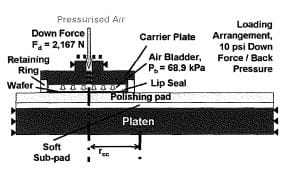
Table 1 Model loading for 10 psi down force, 10 psi back pressure, and 6 psi down force, 4 psi back pressure preset loading configurations on the Westech 372M tool

The carrier and platen shafts were fixed for the model with axial displacement components Ux = Uy= Uz=O. The Uy constraint had to be relaxed on the carrier shaft when the loads Fd and Pb were applied. These loads were simultaneously applied for the equilibrium of the carrier plate in the simulation since the FEM would not converge in the absence of either load. Contact interactions take place between the wafer and the polishing pad as well as
between the retaining ring and the polishing pad. The ABAQUS/Standard ‘hard’ contact algorithm was used to model these interactions, minimizing the penetration of the wafer and retaining surfaces into the polishing pad surface [17].This is a valid assumption for contact of a rigid body with a compliant body such as the wafer and polishing pad, respectively, where the modulus of elasticity of the wafer is three orders of magnitude higher than that of the pad.
This contact model simulated dry solid-solid contact between the pad and the wafer which corresponds directly to the conditions under which the contact pressure measurements are made. In the CMP process itself these simulations conditions are useful under conditions of low platen rotational velocity and relatively high pressure [8]. The wafer was constrained at its edge to be in ‘tied’ contact with the lip seal. The model components were meshed using fully integrated C3D8 3D, eightnode brick elements. A high mesh density was selected such that 93 nodes or data points were generated across the wafer diameter. The selection of this evenly distributed mesh density across the wafer allowed the modelling of the entire wafer surface such that the effect of adjusting the wafer loading at the wafer edge could be seen on the full wafer scale rather than merely the area in which the modification is made.
3.1 Model geometry
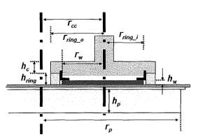
The model components and dimensions are shown in Fig. 2 and are listed in Table 2. The polishing pad and sub pad have a radius of 300 and 285 mm, respectively. The Westech machine was configured with a default ‘polish’ position of the wafer carrier with respect to the platen centre. At this position, the separation distance between the centreline of the wafer carrier and the platen, reo was 76mm, as marked in Figs 1 and 2. The model was configured accordingly with the same value of r cc so that there could be direct comparison with the pressure measurements taken
Table 2 Key dimensions of model components for the 200 mm wafer model

on the machine. The polishing pad and sub pad thicknesses were measured to be 2.68 mm and 1.33 mm for the pad and sub pad respectively.
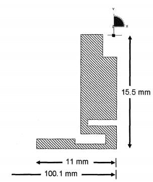
The lip seal has a particularly intricate geometry, as shown in Fig. 3. The effect of the compressed air inside the bladder was modelled by a pressure acting on the inner walls of the lip seal, the underside of the steel carrier plate, and the backside of the wafer within the lip seal. The edge lip of the lip seal was in tied contact with the 5 mm edge ring of the wafer such that contact was maintained throughout the analysis in this region. The effect of sliding friction was also considered between the inner lip of the lip seal and the wafer, assuming a wafer coefficient of friction of 0.01 as reported by Philipossian and Olsen [18).
3.2 Material properties
The moduli of elasticity of the components in the carrier are particularly important parameters in this model. Tensile test specimens were cut using an ASTM
D412 die from the polishing pad, sub pad, and lip seal to characterize these materials accurately. The condition of these materials corresponded to the condition in which they were tested for the pressure measurements. A value of 210 GPa was assumed for the Young’s modulus of both the carrier plate and the platen and 130 GPa for the Young’s modulus of the thermal-oxide-coated wafer, all in agreement with values used by Sorooshian et al. [19). The Young’s modulus of the retaining ring was measured using the three-point bend EN 2746:1998 British standard test. The value obtained is reported in section 5.1.
4 CONTACT PRESSURE MEASUREMENTS
Discrete measurements of contact pressure are required for validation of the FEM. Hoffmann and Decker [20) presented evidence favouring direct measurement of contact pressure using a two-sheet photosensitive-type pressure sensor rather than the use of tactile electronic scan-type grid sensors. They reported that the accuracy of the tactile sensors was adversely affected by the fact that the sensing elements are arranged in a discontinuous grid, and therefore the Young’s modulus of the sensor is discontinuous and the sensor thus intrudes on the contact between the pad and wafer. Photosensitive pressure sensing film similar to that used by Xin [14) was therefore chosen to measure the contact pressure. The sensor operates by pressing a donor film (designated type A) against a blank sheet calibrated such that the intensity of the colour delivered to the blank receiving sheet reflects the magnitude of the pressure. The measurement resolution obtained is 0.5 mm. The rated accuracy of the film is ± 10 per cent or less [21). The film measures accurately in the range between 50 and 250 kPa.
Discrete measurements were taken on three separate occasions using the extreme-low-pressure film in order to remove any possibility of time-dependent viscoelastic deformation and recovery phenomena occurring in the pad during a subsequent test which would adversely affect the accuracy of the measurement. The wafer was loaded into the wafer carrier on the Westech CMP tool as per standard preparation for a wafer Discrete measurements were taken on three separate occasions using the extreme-low-pressure film in order to remove any possibility of time-dependent viscoelastic deformation and recovery phenomena occurring in the pad during a subsequent test which would adversely affect the accuracy of the measurement. The wafer was loaded into the wafer carrier on the Westech CMP tool as per standard preparation for a wafer polishing cycle. Using the pressure test module on the tool the down force and back pressure were steadily ramped to the desired value for the measurement for validity of comparison to the ABAQUS/Standard FEM, a modelling code used for quasi-static processes. The desired pressure was maintained for 90s to ensure the validity of the continuous pressure analysis mode of the accompanying analysis software when analysing the film [21].
5 RESULTS
5.1 Material properties
Figure 4 shows the variation in Young’s modulus obtained from 12 ASTM D412 tensile test specimens cut from an industry standard polishing pad strained at 30 mm/min using the Hounsfield tensile test machine. The average value of Epact from this data is 380 MPa with a standard deviation of 24.5 MPa. Figure 5 illustrates the variation in Young’s modulus obtained from nine ASTM D412 tensile test specimens cut from an industry standard sub pad strained at 15 mm/min also using the Hounsfield tensile test machine. The average value of Esub_pad from this data is 119.3MPa with a standard deviation of 11.6MPa.
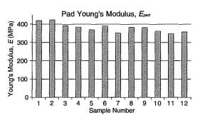
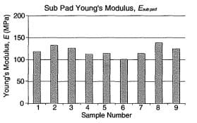
These values represent the effective Young’s moduli of a new, dry pad/ sub pad stack which corresponds to the pad/ sub pad stack used in the measurements of contact pressure reported in section 4.3.
Figure 6 shows the stress-strain curves obtained for six ASTM standard D412 tensile test specimens cut from a rubber lip seal supplied with the wafer carrier on the Westech 372M tool strained at 15mm/min.
Each specimen exhibited variations in cross-sectional area; therefore the maximum and minimum crosssectional area values were used to calculate two stress values for each corresponding strain. The stress-strain curve is clearly non-linear and therefore it was necessary to apply a hyperelastic material model to correctly simulate the deformation behaviour of the seal. Using the material evaluation module in ABAQUS, a 2D polynomial hyperelastic material model was fitted to the averaged test data. Table 3 lists the coefficients determined for the secondorder polynomial governing the stress-strain relationship for the lip seal material. The generalized form of the nth-order polynomial is [17]


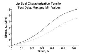
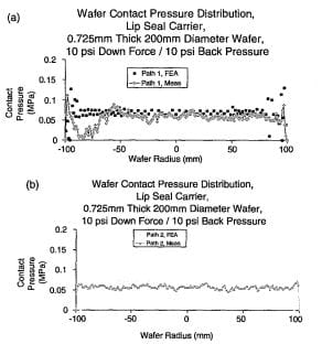
Table 4 Maximum, average, and standard deviation pressures (in MPa) observed in contact pressure distributions from FEM and Prescale film across paths 1 and 2 for 10psi down force, 10psi back pressure loading configuration

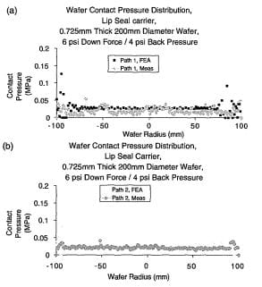
The model predictions and measurement results are compared for another loading configuration, 6 psi down force and 4 psi back pressure, as shown in Figs ll(a) and (b). The results are similarly tabulated in Table 5.
As the polishing pad surface is modelled as a smooth surface with no grooves or surface texture, one would expect that a higher pressure could be recorded in practice than predicted by the FEM at any given point on the wafer, perhaps owing to high local hardness of pad asperities creating localized regions of higher effective pad Young’s modulus and thus creating a high-pressure region between pad and wafer. A close overall correlation is observed in both Figs 10 and 11. The model is thus considered an accurate and robust design tool for optimization of the wafer loading mechanism in CMP
. Incorporating the work of Wang et al. [8], the von Mises stress predicted by the model is considered proportional to the material removal rate resulting from a CMP process performed with these components provided that the rotational speed of the platen is low. The normalized
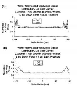
von Mises stress distribution corresponding to Figs 10 and 11, respectively, is shown in Figs 12(a) and (b).
In these normalized distributions, the peak von Mises stress is noted to be 1.732 times (in Fig. 12 (a)) and 2.391 times (in Fig. 12 (b)) the average von Mises stress. Comparing this result to the equivalent value of 4.47 obtained by Wang et al. [8], the differences in the values of pad and sub pad elasticity, the inclusion of the interaction between the retaining ring and the wafer as well as between the pad and the wafer, the inclusion of the effect of the lip seal and air pressure mechanism to pressurize the wafer, and the inclusion of the effect of pad wafer centre separation distance all allows for a more accurate estimation of the polishing performance that would be obtained on the physical machine in actual operation. The loading mechanism modelled by Wang et al. [8] featured a fixed Young’s modulus carrier film in direct contact with the wafer such that all of the down force (7 psi or 48.26 kPa approximately) is transmitted through the carrier film to the wafer. The down force in the presented model is largely transmitted to the retaining ring as the rubber lip seal will not
Table 5 Maximum, average, and standard deviation pressures observed in contact pressure distributions from FEM and Prescale film across paths 1 and 2 for 6 psi down force, 4 psi back pressure loading configuration

carry a significant amount of this load through to the wafer due to its large deformation stress strain characteristic as shown in Fig. 6.Though the work of Wang et al. [8] validated the hypothesis that the form of the normalized stress distribution matches the form of the uniformity obtained in the experiment, the experiment does not validate the model. The comparison of the contact pressure distribution predicted by the FEM and the actual measured pressure distribution of the wafer presented in this paper provides a set of experimental data that can be compared to the static FEM developed herein. Inspection of Figs 10 and 11 does reveal that the comparison is not perfect. The measurements taken with the measurement film are subject to operating pressure range limitations as well as human errors in setting up the test. It is impossible to prepare two identical sets of measurement film for any one test as each set of two sheet film sensors are cut into the shape of the wafer to eliminate the retaining ring contact pressure from the measurement. This ensures that the large deformation induced by the pressure gradient at the inner edge of the retaining ring does not excessively deform the pressure film itself. The orientation of the film as it is scanned for data analysis using a computer is also not repeatable and, as such, the averaging of the measurements taken using the different films scanned are liable to induce some small spatial inconsistencies in the obtained profile. Equally, the global-scale FEM is limited to use of a flat polishing pad surface and thus does not capture the localized phenomena in the pad surface deformation. It is not possible, however, to utilize a local-scale phenomenological model of wafer edge and pad interaction to design an optimum wafer carrier, as such a model would not account for the effect of any design decisions in this small area on the other regions of the wafer.
6 CONCLUSIONS
The FEM predictions demonstrate a correlation to the measured values as highlighted in Tables 4 and 5. The correlation coefficient obtained is 0.55, where a coefficient of one would indicate perfect correlation and a coefficient of zero would indicate no correlation. Inspection of the graphs shown in Figs 10 and 11 suggests that a lot of the pressure measurement points distant from the FEM prediction are higher local pressure peaks. In Fig. 10, a lower average value of contact pressure is observed from the FEM prediction than that of the contact pressure measurements. The absence of a pad surface roughness profile or pad grooves in the model gives rise to a larger contact area than in the measurement setup, and a more consistent radial contact pressure distribution is thus obtained from the model as shown in Figs lO and 11. The fluctuations that take place in the measured profile are generally close to the FEM-predicted values for contact pressure distribution. The pad surface asperity distribution and local hardness phenomena induced by the pad’s deformation under load are thought to cause the observed local peaks in the contact pressure, phenomena that would be difficult to model on the wafer scale. The occurrence of a sufficient number of these local peaks could cause a higher average measured contact pressure than predicted by the FEM in a specific region of the contact zone, as observed in Fig. 10. In inspection of such isolated 2D lines across the wafer, the FEM is a conservative estimate of contact pressure.
The von Mises stress distribution for the wafer is delineated for the 200 mm wafer model and normalized to estimate the anticipated corresponding normalized material removal rate distribution. Notwithstanding some limitations in both the FEM and the contact pressure measuring techniques, as previously discussed, the model is shown to give a robust indication of the anticipated polishing performance of a particular wafer carrier, namely the existing former industry carrier on the Westech 372M 200 mm wafer polisher. The occurrence of a lower contact pressure prediction in the FEM also implies a lower prediction of material removal rate following from the proportionality of removal rate asserted by Preston [1) and by Tseng et al. [2) discussed earlier in this paper. However, the model results compare favourably to the measured contact pressure as evident from the calculated Pearson product moment coefficients of 0.55
The FEM presented here is thus shown to be a suitable design-for-manufacture tool for enhancing wafer carrier design, in particular, to optimize wafer loading. The work presented in this paper also accurately models the two independently applied pressures, namely the load acting on the carrier and the wafer backside pressure, and thus provides a realistic model to allow accurate prediction of the effect of changing these parameters. The measurement of material properties of the polishing pad, sub pad, lip seal, and retaining ring also correspond to the condition corresponding to the experimental setup to remove any uncertainty in the comparison between model and results. Appropriate scaling of the model will next be undertaken to expand the findings of this work to the future 450 mm wafer diameter.
©Authors 2011
REFERENCES
1 Preston, F. W. The theory and design of plate glass polishing machines.]. Soc. Gl
ass Technol., 1927, 11, 214-256.
2 Tseng, W. T., Chin, J, H., and Kang, L. C. A comparative study on the roles of velocity in the material removal rate during chemical mechanical polishing. ]. Electrochem. Soc., 1999, 146, 1952-1959.
3 Bukkapatnam, S., Rao, P., and Komanduri, R. Experimental dynamics characterization and monitoring ofMRR in oxide chemical mechanical planarization (CMP) process. Int.]. Mach. Tools Mf., 2008, 48(12-13), 1375-1386.
4 Che, W., Guo, Y., and Chandra, A. A scratch intersection model of material removal during chemical mechanical planarization (CMP). ]. Mfg Sci. Engng, 2005,127,545-554.
5 Chen, K., Yeh, H. M., Yan, J, L., and Chen, Y. T. Finite-element analysis on wafer-level CMP contact stress: reinvestigated issues and the effects of selected process parameters. Int. ]. Adv. Mfg Technol., 2009, 42(11), 1118-1130.
6 Fu, G. and Chandra, A. The relationship between wafer surface pressure and wafer backside loading in chemical mechanical polishing. Thin Solid Films, 2005, 474(1-2), 217-221.
7 Weber, C., Weiser, J,, Zeidler, D., and Bartha, J, W. Adaptive piezo-controlled carrier for CMP processing. In Proceedings of Materials Research Society Spring Meeting 2004, Symposium K: Advances in Chemical-Mechanical Polishing, San Francisco, CA, April15-19 2004, pp. 81-85.
8 Tseng, W. and Wang, Y. Re-examination of pressure and speed dependences of removal rate during chemical mechanical polishing processes. ]. Electrochem. Soc., 1997, 144, Ll5.
9 Byrne, G., Mullany, B., and Young, P. The effect of pad wear on the chemical mechanical polishing of silicon wafers. CIRP Ann.-Mjg Technol, 1999, 48(1), 143-146.
10 Lin, Y. Y. and Lo, S. P. A study of a finite element model for the chemical mechanical polishing process. Int.]. Adv. Mfg Technol., 2004, 23(9), 644-650.
11 Lo, S., Lin, Y., and Huang, J, Analysis of retaining ring using fmite element simulation in chemical mechanical polishing process. Int. ]. Adv. Mfg Technol., 2007, 34(5), 547-555.
12 Yao, L, Kirkpatrick, M., Kalenian, B., Sennett, B., and Spiegel, L CMP enhancement applications using VIPRR carrier technology. In Proceedings of SEMICON China, Shanghai, March 21-23, 2006, SEMI: China.
13 Chiu, J, and Lin, Y. Modal analysis of multi-layer structure for chemical mechanical polishing process. Int.]. Adv. Mfg Techno[., 2008, 37(1), 83-91.
14 Xin, Y. Modeling of pad-wafer contact pressure distribution in chemical-mechanical polishing. Int. ]. Mfg Sci. Technol., 2000, 2(1), 20–33.
15 Xia, X. and Ahmadi, G. Surface removal rate in chemical-mechanical polishing. Part. Sci. Technol., 2002, 20(3), 187-196.
16 Rike, D. A. Planar downforce BKM’s-downforceforce on pad, Intel, 2007.
17 Simulia. ABAQUS/CAE version 6.7 Users Manual Version 6.7, Simulia, 2009.
18 Phllipossian, A. and Olsen S. Effect of pad surface texture and slurry abrasive concentration on tribological and kinetic attributes of ILD CMP. In Proceedings of Materials Research Society Spring Meeting, 767, pp. 119-126, Santa Clara, CA, 2003.
19 Soroosbian, J., Phllipossian, A., Goldstein, M., Beaudoin, S., and Huber, W. Impact of wafer geometry and thermal history on pressure and von Mises stress non-uniformity during chemical mechanical planarization. Jpn.]. Appl. Phys., 2003, 42, 6363-6370.
20 Hoffmann, K. and Decker, K. Inaccuracies in measurement of contact pressure due to the measuring grid of a foil sensor. Int.]. Intell. Syst. Technol Appl., 2008, 3(1/2), 80-94.
21 Fujifilm. Fujifilm pressure distribution mapping system for Prescale, edition 2.01, Fuji, 2008.


