Sung-Won Youn*, Mayuko Ogiwara, Hiroshi Goto, Masaharu Takahashi, Ryutaro Maeda
Advanced Manufacturing Research Institute, National Institute of Advanced Industrial Science and Technology (AIST), 1-2-1 Namiki, Tsukuba, Ibaraki 305-8564, Japan
Abstract
In this study, the prototype of a thermal roller imprint lithography (RIL) system was developed and applied to RIL tests to evaluate its feasibility for the large area replication of an optical micro device. The developed system adapts an automatic stamp releasing mechanism and has the capacity to replicate ultra-precision structures on an area of 100mm × 100mm at the scanning speed range of 0.1–10 mm/s. For RIL tests, 1mm-thick polyethylene terephthalate (PET) plastic plates and 100 ¨m-thick cycloolefin resin filmswere used as imprint materials. All samples were 100mm×100mmin size. The combination of a thin and flexible polymer film and an elastomeric adhesive sheetwas effective for both rapid processing and uniform replication. For given RIL conditions (700N press force and Tg +50°C roller temperature), the complete filling for a 1 mm-thick PET sample was achieved at the roller scan speeds of 0.1 mm/s, whereas that for a 100 ¨m-thick cycloolefin sample could be obtained at the roller scan speeds of < 2mm/s with much better replication uniformity over a whole surface area. Finally, a light guide plate (LGP) for a back light panel was fabricated by RIL.
1. Introduction
Since the mid-1990s, imprint lithography has drawn a lot of attention as one of the most promising technologies for the definition of nano/micro-patterns due to its simplicity, low cost and high resolution (Chou et al., 1996; Gates et al., 2005; Guo, 2004; Guo et al., 2004; Heidari et al., 2000; Nakajima et al., 2006; Scheer and Schulz, 2001; Torres et al., 2003; Chang et al., 2006; Seo et al., 2007; Youn et al., 2007). One of the current key issues of this lithography technique is the size of a processing area, since it is one of the major factors that dominate the process throughput. The need for rapid and uniform patterning over a large area has lead to the development of a number of imprint-based technologies such as an imprint lithography using a flat-type stamp with a large surface area (Heidari et al., 2000; Scheer and Schulz, 2001), a step-and-stamp imprint lithography (SSIL) (Gates et al., 2005; Guo, 2004; Torres et al., 2003) roller imprint lithography (RIL) (Chang et al., 2006; Seo et al., 2007; Suh et al., 2005; Tan et al., 1998) and others. Among those technologies, traditional flat imprint lithography using a large stamp is the simplest way, but commonly requires several tons of force that increases the possibility of stamp deformation. Further, the thickness variation on a stamp or substrate can be as large as a micrometer on a large wafer area, and it is hard to be compensated (Heidari et al., 2000). During imprinting, non-conformal contact occurred by the local flatness distortion in the mold causes the reduction of replication uniformity and leads to a huge stress concentration, resulting in the warping or distortion of the stamp (Deguchi et al., 2002; Lazzarino et al., 2004). In the SSIL process, a stamp is pressed into a polymer film under suitable pressure and temperature conditions replicating the pattern in the stamp into the polymer, followed by stepping to the adjacent site. Thus, the SSIL is not the best choice for the replication of continuously connected and complex-shaped structures such as micro-channels for bio-devices although it can transfer nano/micro-scale patterns over large areas. The RIL, first proposed by the Chou group (Tan et al., 1998), is one of the most promising candidates for rapid patterning on a very large area substrate. As compared to other two types of large area replication methods previously described above, the RIL process provides some distinctive advantages (e.g, compact-sized system configuration, lower imprint force, better replication uniformity) because only a line area is in contact during imprinting. The line contact between the stamp and polymer surfaces during imprinting reduces the force for the complete filling, the effects of thickness unevenness and dust. Moreover, the RIL has more flexibility in the choice of replication geometry. Up to date, several kinds of RIL techniques (e.g, rollto- roll (Seo et al., 2007; Suh et al., 2005), roll-to-plate (Chang et al., 2006) and others) have been studied by several research groups, but have been generally limited to ultra-violet (UV) -based techniques.
The aims of this study are to develop the prototype of a roll-to-plate type thermal-RIL system and to evaluate its feasibility for the large area replication of an optical micro device, such as a light guide plate (LGP) for a back light panel. The back light panels with a LGP provide features of high brightness, high uniformity, thin and lightweight, and are widely used on various applications for monochrome and color displays. Series of RIL tests were conducted to investigate the effects of process conditions (e.g, scan speed of roller, vertical press force and temperature) on the formability of polymer materials including a polyethylene terephthalate (PET) and a cycloolefin resin. For comparison, flat imprint tests were also performed. Polyethylene terephthalate (PET) plastic and two types of polyolefin resins were used as imprint materials. Finally, LGPs were replicated under the achieved process conditions by the RIL.
2. Experimental procedure
Commercially available thermoplastic polymers, including polyethylene terephthalate (PET Tg = 81.5 °C) plastic and two types of polyolefin resins (product name of “Zeonoa ZF14-100” and “Zeonex”), were used as imprint materials. Zeonoa and Zeonex are new thermoplastic polyolefin resins (cycloolefin polymers) developed by Zeon Corporation and have almost the same glass transition temperature of about 138 °C. Series of RIL tests were conducted on a 1 mm-thick PET plastic plate and a 100 um-thick Zeonoa resin film using the prototype of a RIL system thatwas developed in this study. The details regarding the development of RIL system are described in the next section All samples used for RIL tests were 100mm × 100mm in size. To fix the sample film (or plate) on the sample platform in the RIL system (refer Fig. 2 (a)), a heat-resistant silicone rubber adhesive sheet (product name of “Hi Performance Stickiness Plate (HSP)”, Shin-Etsu Polymer Co. Ltd., Japan) film was used. Flat imprint tests on 1 mm-thick PET and 2 mm-thick Zeonex plates were also performed in hot-press equipment, which is designed to imprint 3 cm × 3 cm samples (the maximum heating temperature: 700 °C and the maximum press force: 2 kN). A pumping system allows embossing samples under vacuum, with the pressure of 1 Pa inside the chamber. Prior to imprint tests, local flatness distorti
ons in the mold were evaluated using a pressure-sensitive film (Prescale film, Fuji- Film Co., Japan), and compensated. No mold release agentwas used. For roller and conventional imprint tests, three types of nickel micro-molds were prepared. The fabrication process of a nickel mold began with silicon micromachining process, such as deep reactive ion etching (RIE) using standard Bosch process. After sputtering seed and barrier metallic layers on the silicon master, nickelwas electroplated to sufficient thickness. In the final step, the silicon master was etched away using KOH-based solution after chemical mechanical planarization (CMP) of the backside of the electroplated nickel. An optical microscope and a conforcal microscope were used to obtain the local morphological data of the processed samples. The commercial macro observation system for micro-scale defect detection (Geoscan, Japan minicomputer systems Co. Ltd., Japan) was also utilized to evaluate the replication uniformity over a whole sample surface area. This system enables to visualize the micro-scale defects over the whole surface area of a wafer by detecting the change of a specular reflection
3. Results and discussion
3.1. Development of roller imprint lithography (RIL) system
Fig. 1 shows the photograph of the developed RIL system hardware. The system is made up of the major components such as a roller imprint system, a control system, a control panel, and computer for test conditions input and data acquisition.
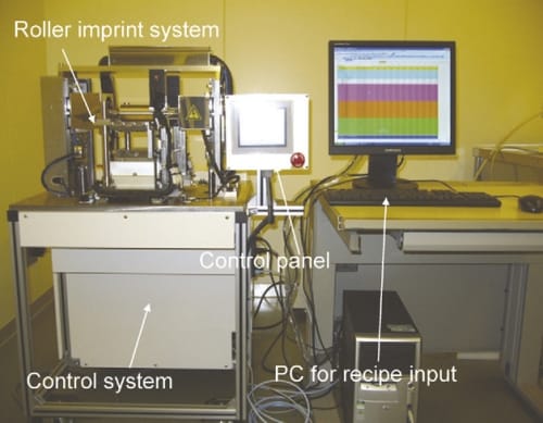
Fig. 1 – An overview of the system hardware.
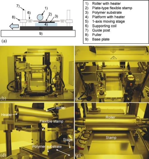
Fig. 2 – (a) Schematic diagram and (b–e) photographs of the roller nano/micro-imprint lithography system.
Fig. 2 shows the schematic diagram and photographs of the roller nanoimprint system consisting of major components such as the air–cylinder-actuated roller press device with heaters, the one-axis moving stage with a heater, and the automatic stamp release mechanism. The automatic stamp releasing mechanism was adapted in the system because it was considered that the automatic and quick removal of stamp is efficient to reduce the pattern distortion resulting from the difference in the shrinkage amount between the stamp and the substrate. The sample platform can travel, parallel to the sample surface, at the speed range of 0.1–10 mm/s. The maximum distance allowed for the substrate travel is about 120mm. The maximum press force capacity for the system is 2 kN with a precision of less than micro-Newton. The press force and the scan speed of roller are controlled by a control system (Fig. 2). The detailed specification of the system is summarized in Table 1.
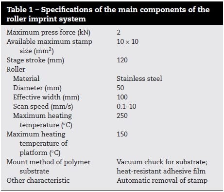
Table 1 – Specifications of the main components of the roller imprint system
The major process flow for the RIL is depicted in Fig. 3. Process starts with mounting a polymer sample on the bottom platform. Then, the plate-type flexible stamp supported by several coils (refer Fig. 2 (a))moves down to contact with the surface of polymer substrate, and both a roller and a platform are heated to set temperature. Commonly, the roller temperature is set above the glass transition temperature (Tg) of the polymer substrate, while the temperature of the platform is set below the Tg because the stamp is heated by the heat conduction from the roller. In rolling, the roller is rotated over the stamp and the slight deformation of the stamp under the pressure of the roller allows imprinting in polymer substrate.Next, the polymer substrate mounted on amoving stage moves parallel, applying the vertical press force to the sample’s surface by the roller. The press force on the sample is controlled and can be held constant, increased, or decreased at a linear rate. Simultaneously, pullers move along the z direction to remove the stamp from the polymer substrate automatically. After completing a RIL process, the stamp returned to the initial position.
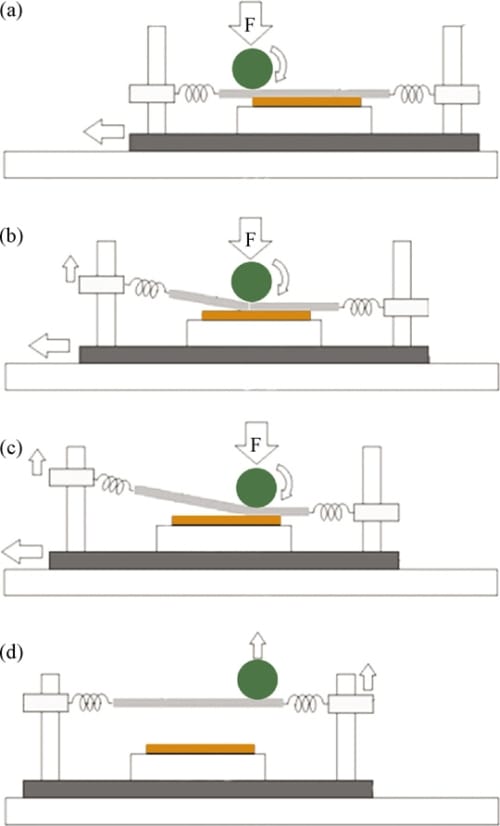
Fig. 3 – Process layout of the modified roller nano/micro-imprint lithography; (a) the plate-type flexible stamp supported by several coils moves down to contact with the surface of polymer film for heating and imprinting, (b and c) The roller is rotated over the stamp, and the sample stage moves parallel, applying the vertical press force to the sample’s surface by the roller. Simultaneously, pullers move along the z direction to remove the stamp from the polymer film automatically. (d) The stamp returned to the initial position.
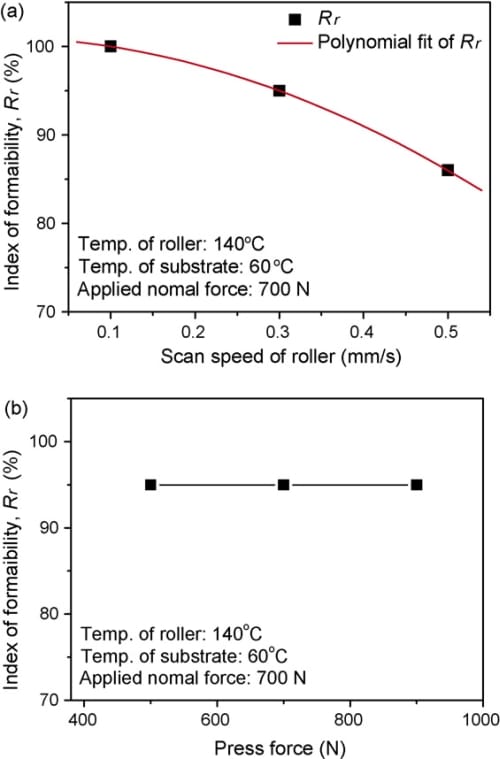
Fig. 4 – Relationships between the formability of PET plastic and the process parameters including (a) the scan speed of roller and (b) the press force.
3.2. Roller and flat imprint tests
In order to evaluate the feasibility of the developed RIL system for a large area replication, series of imprint tests were performed by varying process parameters. Proper RIL conditions are crucial because the polymer may not fully deform during imprinting at a fast scan speed or at low press force, depending on the temperature (or polymer viscosity).
Imprint tests for 1 mm-thick PET samples were carried out under the different press force and roller scan speed using a 0.3 mm-thick nickel stamp (data is not included). Temperatures of the roller and the platform were set at 140 °C (e.g., higher than 50 °C for the Tg of PET) and 60 °C, respectively. The appearance and morphologies (such as dimensions) of the stamp and processed sample surfaces were observed and measured using an optical microscope and a conforcal type microscope. From these morphological analyses, the evaluation index of formability was calculated as a percentage of replicated height Rr = Hr/Hs, where Hr and Hs are the height of replicated structure and the depth of master structure, respectively. The relationship between the formability of a PET material and the process parameters (e.g, scan speed of roller and press force) are shown in Fig. 4. Under the press force of 700N, index Rr increased from 86 to 100% with the decrease of the scan speed from 0.5 to 0.1 mm/s. Additionally, under the scan speed of 0.3 mm/s, index Rr did not vary regardless of the press force increase from 500 to 900N.
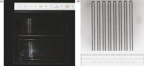
Fig. 5 – (a) Photograph of a typical PET sample (size: 100mm × 100mm) after imprint test. The surface is composed of the array of 0.8–5 μm-wide and 1 μm-deep microstructures. (b) The image achieved using conforcal microscope showing array of 4 μm-wide and 1 μm-deep lines with 4 μm spacing (magnification of (a)).
One example of replication results is represented in Fig. 5. Good replication of mixed structures (Rr = about 95%) with sizes ranging from 800nm up to 5 ¨m (depth: 1 ¨m) over the whole surface area was obtained under the condition of 500N of press force, 0.3mm/s of scan speed and 140 °C of roller temperature.
A nickel stamp for the replication of LGP was prepared by a silicon micromachining process, followed by an electroplating process. Fig. 6(a) shows the photograph of the fabricated nickel mold with 100mm × 200mm size and 0.3mm thickness. As shown in Fig. 6(b) and (c), the surface of nickel mold is composed of numerous 38 ¨m-wide, 63 ¨m-long and 8.5 ¨m-high microstructures
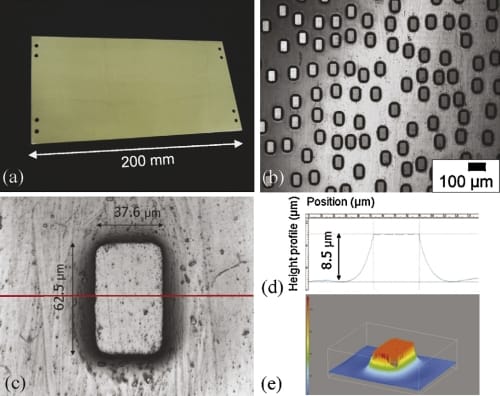
Fig. 6 – (a) Photograph flexible nickel stamp (100mm×200mm) for the replication of a light guide plate (LGP) for back light panel and (b) its optical magnification image. (c) Optical micrograph, (d) surface profile and (e) 3D image of the nickel master microstructure achieved using a conforcal microscope.
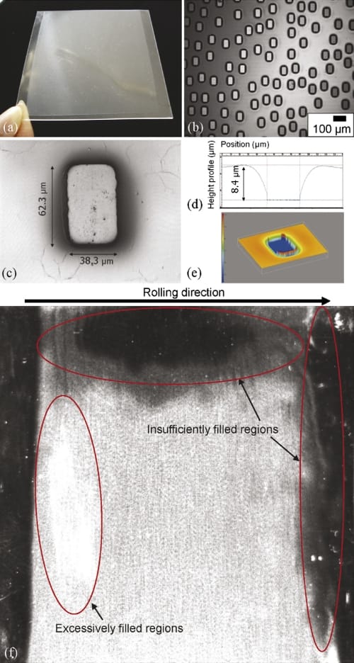
Fig. 7 – (a) Photograph of 1 mm-thick PET sample (100mm×100mm) after RIL tests under the condition of less than 700N of press force, 0.3mm/s of scan speed and 140 °C of roller temperature and (b) its magnification. (c) Optical micrograph, (d) surface profile and (e) 3D image of the nickel master microstructure achieved using a conforcal microscope. (f) The image achieved using the Geoscan. The whole surface area of 100mm×100mm is represented with defects.
In Fig. 7, a 1 mm-thick PET plate with 100mm×100mm size was imprinted for the replication of a light guide plate under the condition of 700N press force, 0.3mm/s scan speed and 140 °C roller temperature, and its surface was observed by an optical microscope, a conforcal microscope and a macro observation tool for micro-scale defect detection. Although complete fillingwas achieved in the middle area of the sample, the replication uniformity at the peripherywas not acceptable, indicating that the parallelism between the stamp and the PET sample plate was not enough for contacting the entire surface of stamp and sample plate.
RIL tests on 100 ¨m-thick cycloolefin resin films were carried out by decreasing the scan speed of the roller incrementally from 7 to 1mm/s at different roller temperatures of 170, 190 and 210 °C. The temperature of the platform was set at 125 °C. The investigated relationship between the formability of a 100 ¨m-thick cycloolefin resin film and the process parameters including the scan speed of the roller and the temperature are shown in Fig. 8. Under the press force of 700Nand the roller temperatures of 190 and 210 °C, the complete filling for the 1 mm-thick PET plastic plate was achieved at the roller scan speeds of 2 mm/s.
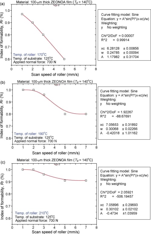
Fig. 8 – Relationships between the formability of cycloolefin resin films and the process parameters including the temperature and the scan speed of roller.
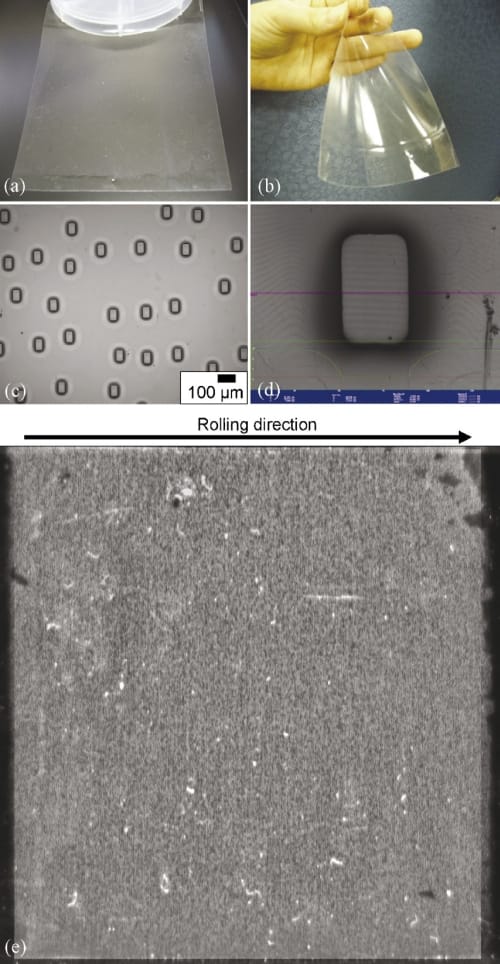
Fig. 9 – (a and b) Photographs of 100 μm-thick cycloolefin (Zeonoa) resin films imprinted under the condition of less than 700N of press force, 1mm/s of scan speed and 190 °C of roller temperature. (c) Micrographs obtained using a conforcal microscope and its magnification (d). (e) The image achieved using the Geoscan. The whole surface area of 100mm × 100mm is represented with defects.
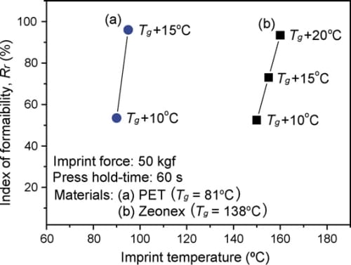
Fig. 10 – Relationships between the formability of imprint materials (e.g., PET plastic and cycloolefin (Zeonex)) and the imprint temperature.
In Fig. 9, a 100 ¨m-thick cycloolefin resin film with 100mm × 100mm size was imprinted for the replication of a LGP under the condition of 700N press force, 1mm/s scan speed and 190 °C roller temperature, and its surface was observed by an optical microscope, a conforcal microscope and a macro observation system. As can be seen in Fig. 9(c) and (d), 38 ¨m-wide, 63 ¨m-long and 8.5 ¨m-deep microstructures could be replicated with good fidelity. The macro-image obtained using the Geoscan (Fig. 9(e)) represented the apparently better replication uniformity over the whole surface area, as compared to that of Fig. 7.
It should be noted that the intrinsic characteristics of both materials (e.g., PET plastic and cycloolefin resin) is not the major factor that enabled the faster and more uniform replication of cycloolefin samples. For better understanding, flat imprint tests were also performed on 1 mm-thick PET and 2 mm-thick cycloolefin (Zeonex) plates, and the change of their formability in accordance with the temperature was measured as shown in Fig. 10. The used nickel mold was 25mm × 25mmin size, and its surfacewas composed of arrays of 1 ¨m-high and 1 ¨m-wide lines with 1 ¨mspacing. One distinctive fact is that the PET sample showed better formability than the cycloolefin (Zeonex) sample in the flat imprint tests at Tg + 15°C.
4. Conclusions
From the preceding considerations, it was considered that the combination of an elastomeric adhesive sheet and the thin and flexible resin film would provide better conformal and larger contact (between the stamp and resin film surface) during the rolling process because both a sheet and a film are flexible and thus they can be more easily bent or deformed by the externally applied force, allowed for faster complete filling and better uniformity over the whole surface area.
Acknowledgements
In summary, the prototype of a thermal roller imprint lithography (RIL) system was developed and applied to RIL tests to evaluate its feasibility for the large area replication of the MEMS device. The developed system adapts an automatic stamp releasing mechanism and can replicate ultra-precision structures on the area of 100mm × 100mm at the scanning speed range of 0.1–10 mm/s. For RIL tests, 1 mm-thick polyethylene terephthalate (PET) plastic plate and 100 ¨mthick cycloolefin (Zeonoa) resin film were used as imprint materials. All samples were 100mm × 100mm in size. For given RIL conditions (700N press force and Tg + 50 °C roller temperature), the complete filling for a PET sample was achieved at the roller scan speeds of 0.1 mm/s, whereas that for a cycloolefin sample could be obtained at the roller scan speeds of < 2mm/s with much better replication uniformity over a whole surface area. Contrarily, in the flat-imprint tests at Tg + 15°C, PET showed better formability than cycloolefin (Zeonex). These results suggested that the combination of a thin/flexible polymer film and an elastomeric adhesive sheet was the most major reason for rapid processing aswell as uniform replication. Lastly, the light guide plate (with a surface composed of numerous 38 ¨m-wide, 63 ¨m-long and 8.5 ¨mdeep microstructures) for back light panel was fabricated by RIL. Obtained replication results indicated that the developed RIL system is suitable for the fabrication of various optical micro devices such as flat panel displays, electronic papers, functional films, and others.
References
- Chang, C.Y., Yang, S.Y., Sheh, J.L., 2006. A roller embossing process for rapid fabrication of microlens arrays on glass substrates. Microsyst. Technol. 12, 754–759.
- Chou, S.Y., Krauss, P.R., Renstrom, P.J., 1996. Nanoimprint lithography. J. Vac. Sci. Technol. B 14 (6), 4129–4133.
- Deguchi, K., Takeuchi, N., Shimizu, A., 2002. Evaluation of pressure uniformity using a pressure-sensitive film and calculation of wafer distortions caused by mold press in imprint lithography. Jpn. J. Appl. Phys. 41, 4178–4181.
- Gates, B.D., Xu, Q., Stewart, M., Ryan, D., Willson, C.G., Whitesides, G.M., 2005. New approaches to nanofabrication: molding, printing, and other techniques. Chem. Rev. 105, 1171–1196.
- Guo, L.J., 2004. Recent progress in nanoimprint technology and its applications. J. Phys. D: Appl. Phys. 37, R123–R141.
- Guo, C., Feng, L., Zhai, J., Wang, G., Song, Y., Jiang, L., Zhu, D., 2004. Large-area fabrication of a nanostructure-induced hydrophobic surface from a hyd
rophilic polymer. Chem. Phys. Chem. 5, 750–753. - Heidari, B., Maximov, I., Montelius, L., 2000. Nanoimprint lithography at the 6 in. wafer scale. J. Vac. Sci. Technol. B 18 (6), 3557–3560.
- Lazzarino, F., Gourgon, C., Schiavone, P., Perret, C., 2004. Mold deformation in nanoimprint lithography. J. Vac. Sci. Technol. B 22 (6), 3318–3322.
- Nakajima, M., Yoshikawa, T., Sogo, K., Hirai, Y., 2006. Fabrication of multi-layered nano-channels by reversal imprint lithography. Microelectron. Eng. 83, 876–879.
- Scheer, H.-C., Schulz, H., 2001. A contribution to the flow behaviour of thin polymer films during hot embossing lithography. Microelectron. Eng. 56, 311–332.
- Seo, S.-M., Kim, T.-I., Lee, H.H., 2007. Simple fabrication of nanostructure by continuous rigiflex imprinting. Microelectron. Eng. 84, 567–572.
- Suh, D., Choi, S.-J., Lee, H.H., 2005. Regiflex lithography for nanostructure transfer. Adv. Mater. 17, 1554–1560.
- Tan, H., Gilbertson, A., Chou, S.Y., 1998. Roller nanoimprint lithography, 1998. J. Vac. Sci. Technol. B 16 (6), 3926–3928.
- Torres, C.M.S., Zankovych, S., Seekamp, J., Kam, A.P., Cedeno, C.C., Hoffmann, T., Ahopelto, J., Reuther, F., Pfeiffer, K., Bleidiessel, G., Gruetzner, G., Maximov, M.V., Heidari, B., 2003. Nanoimprint lithography: an alternative nanofabrication approach. Mater. Sci. Eng. C 23, 23–31.
- Youn, S.W., Takahashi, M., Goto, H., Maeda, R., 2007. Fabrication of micro-mold for glass embossing using focused ion beam, femto-second laser, eximer laser and dicing techniques. J. Mater. Process. Technol. 187/188, 326–330.


