George A. Riley, PhD
FlipChips Dot Com
A recent conference paper showed the advantages of a pressure-indicating film in wafer-to-wafer bonding (Ref 1). The film may have similar advantages for several applications in flip chip assembly.
Placing Pressurex® film between two surfaces causes it to change color in direct proportion to the local pressure applied, giving an irreversible “pressure footprint” of the surface. The pressure magnitude at any point may easily be determined by comparing the color to a calibrated color correlation chart, analogous to using litmus paper to determine acidity.
Figure 1 shows a color map of a wafer and its pressure interpretation. Visual comparison gives ±10% accuracy in determining pressure. An optical measurement system increases accuracy to ±2%.
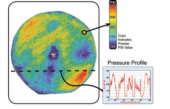
Figure 1. Wafer pressure footprint and interpretation.
The success of Pressurex® film in wafer bonding suggests similar applications in flip chip assembly, where pressure magnitude and spatial uniformity may be critical. This is particularly likely with large die, which are becoming more common. Die larger than 20mm square, with more than 25,000 bumps per die, are already in routine production (Ref 2).
Potential pressure sensing applications include die-to-substrate coplanarity, bump coining for uniform bump heights, and several pressure-sensitive bonding methods.
Coplanarity
Successful flip chip assembly of large die with many bumps for applications such as image sensors depends upon the substrate and the die that is being placed upon it having parallel, coplanar surfaces when they are brought in contact. Any deviation from coplanarity can cause open or poor electrical connections. Extreme cases may misalign the die by imparting a sideways sliding motion during placement pressure, or may even crack the die. Figures 2 and 3 show some potential effects of non-coplanar bonding (Ref 3).

Figure 2. Misalignment may create acceptable bonds on side A, but open
circuits from failures to bond on side B.
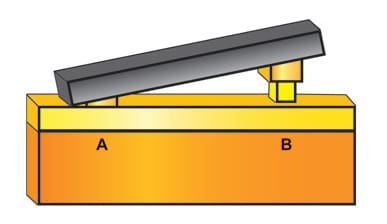
Figure 3. Misalignment may create short circuits on side A due to
overpressure, and acceptable bonds on side B.
Conventional approaches for establishing and verifying coplanarity depend upon optical or laser equipment. However, most flip chip bonders do not have either of these expensive add-ons. Without them, establishing coplanarity often requires repeated trial-and-error planarity adjustments using sample assemblies and microscopic inspection.
Coining
Gold stud bump flipchip assembly (Tutorial 3) places gold bumps on the die using a modified wire bonder. As deposited, those bumps have wire tails of varying length, as well as variations in bump height. Figure 4 shows a bump as deposited.
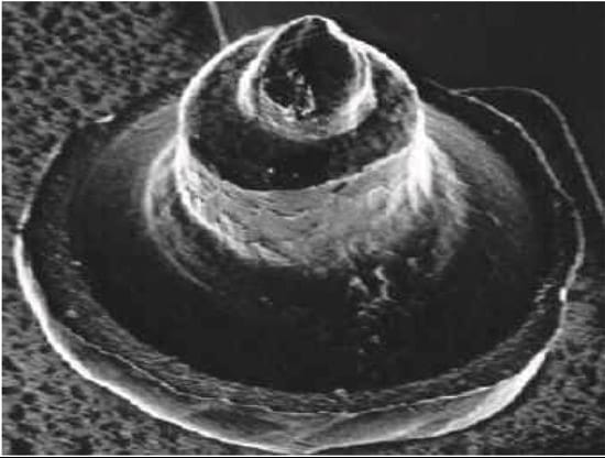
Figure 4. Gold stud bump, showing wire stub at top.
“Coining” by pressing the bumped die against a flat surface is a common method to reduce height variations and create larger contact areas. Figure 5 is a cross-section of a coined bump. Again, inadequate or non-uniform pressure across the die surface may cause some bumps to have varying heights, causing open or poor contacts. Pressure-sensing film would verify uniform bump height.
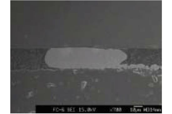
Figure 5. Cross-section of a coined gold stud bump connection.
Bonding
Many common methods of flip chip bonding require controlled, uniform pressure to avoid opens, poor contacts, and die cracking:
-
- Thermosonic bonding experiments found an optimum pressure for best bond adhesion. Higher or lower pressures gave poorer bond shear results (Tutorial 9). (Ref 3).
-
- Thermocompression bonding requires higher bonding pressures than thermosonic, raising the consequences of inadequate pressure control. Copper/Copper thermocompression bonding of copper “nails” on a die to copper bond pads on a wafer has been demonstrated for high density 3D assemblies (Ref 4).
-
- Copper/Tin interdiffusion bonding of chips to wafers in 3D heterogeneous assemblies depends upon proper pressure at 300°C to form a stable copper-tin intermetallic, with copper upper and lower bonding surfaces. (Ref 5)
- Gold/Tin wafer bonding tests show that too much pressure causes squeeze-out of solder, potentially leading to open or short circuits. Non-uniform pressure may squeeze solder out in some areas, but not in others (Ref 1). The same problem could occur with large die in chip-to-substrate or chip-to-wafer Gold/Tin bonding.
In conclusion, the performance of Pressurex® film in wafer bonding and the importance of quality control in all of the above assembly examples suggest that film pressure sensing could significantly improve flip chip assembly yield, costs, and set-up time.
References
- D. Spicer et al, Pressure Indicating Film Characterization of Pressure Distribution in Eutectic Au/Sn Wafer-to-Wafer Bonding, Proceedings International Wafer-Level Packaging Conference, pp. 135 – 139, October 27 – 30, 2009.
- R. Asgari, Copper Pillar and Micro Bump Inspection Requirements and Challenges, Proceedings International Wafer-Level Packaging Conference, pp. 186 – 188, October 27 – 30, 2009.
- L.K. Cheah et al, Gold to Gold Thermosonic Flip-Chip Bonding, Proceedings HDI 2001, April 2001, pp 165 – 175. See also Tutorial 9 .
- P. De Moor et al, “Recent Advances in 3D Integrations at IMEC,” MRS Fall Meeting, November 27 – December 1 2006,Boston. See also Tutorial 71 .
- M. Jurgen Wolfe, et al, Technologies for 3D Heterogeneous Integration, Proceedings of SMTA Pan Pacific Symposium 2008. See also Tutorial 90


