He Gao, Hua Tan, Wei Zhang, Keith Morton, and Stephen Y. Chou*
Nanostructure Laboratory, Department of Electrical Engineering,
Princeton UniVersity, Princeton, New Jersey 08544
Abstract
Imprint pressure uniformity is crucial to the pattern uniformity and yield of nanoimprint lithography (NIL) and, hence, its applications. We studied a novel imprint method, air cushion press (ACP), in which the mold and substrate are pressed against each other by gas pressure rather than solid plates, and compared it with a common method, solid parallel-plate press (SPP). We found that (a) under normal imprinting conditions the measured pressure distribution across a 100-mm-diameter single imprint field in ACP is nearly an order of magnitude more uniform; (b) ACP is immune to any dust and topology variations on the backside of the mold or substrate; (c) when a dust particle is between the mold and substrate, ACP reduces the damage area by orders of magnitude; (d) ACP causes much less mold damage because of significantly less lateral shift between the mold and substrate; and (e) ACP has much smaller thermal mass and therefore significantly faster speed for thermal imprinting.
Nanoimprint lithography (NIL)1,2 has demonstrated the ability to pattern 5-nm-line-width and 6-nm-half-pitch features3,4 and replicate features with high fidelity over a large patterning area.5 Among all nanopatterning techniques, NIL offers a unique combination of ultrahigh resolution, low cost, and high throughput and has been applied to a broad range of disciplines.6-8 Recently, NIL has been placed on the International Technology Roadmap for Semiconductors (ITRS) as next generation lithography (NGL) for semiconductor IC manufacturing.9
NIL creates patterns by physically deforming a material (a polymer resist or a functional material) with a mold; hence, it requires an intimate contact between the mold and substrate, which, in turn, requires a uniform imprint pressure everywhere over the entire imprint field. Moreover, to reduce damage to the mold and prolong mold lifetime, one should avoid high pressure points over the imprint field and any relative rotation and lateral shift between the mold and substrate during imprint processes. To meet these requirements, innovative imprint pressing methods are needed.
One commonly used pressing method for imprint is the solid parallel-plate press (SPP) (Figure 1a). SPP is simple to construct and is often used in home-built NIL tools as well as many commercial NIL machines. However, SPP suffers several drawbacks: (1) any roughness, nonflatness, or dust on the surface of a press plate (Figure 1b) and/or the backside surface of the wafer and the mold (Figure 1c) will cause nonuniform pressure distribution, which results in imprint nonuniformity and local high pressure points that will damage the mold and/or substrate; (2) the two press plates may not be perfectly parallel with each other (Figure 1d), and hence assert shear and/or torque forces, causing relative shift and/or rotation between the mold and substrate; 10 (3) if either the mold and/or substrate has curved surfaces, then SPP could not bring all of the mold and substrate surfaces in contact, leaving a large fraction of the wafer area unimprinted, (Figure 1e); (4) in SSP, because a constant force is applied between the two plates to provide the desired pressure, if the mold and substrate surfaces are in contact only at a point or in a small area, then an enormous pressure can be generated at this contact point or area, causing damages to the mold or substrate; and (5) the parallel plates of SSP have large thermal mass, making isothermal NIL processing time unduly long. The nonconformal contact and nonuniform pressure in SPP will result in undesired gaps between the mold and substrate in certain areas of the sample, which in turn lead to no imprint, or regions of very thick resist (if the resist can flow to the gap) that prevent imprinted nanopatterns from being transferred to the substrate, or some chaotic patterns due to liquid instability.11
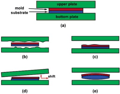
Figure 1. Schematics of the solid parallel-plate press (SPP) nanoimprint method and drawbacks: (a) ideal SPP; (b) imperfect plate surfaces; (c) uneven mold/substrate backside; (d) nonparallelism between plates; and (e) curved sample surfaces.
Air Cushion Press (ACP) for Imprinting. To improve pressure uniformity, yield, and thermal imprint speed, and to overcome the aforementioned issues, a new technique, air cushion press (ACP) (Figure 2), has been developed.12 ACP utilizes a gas (or fluid) to press the mold and substrate against each other in a chamber. ACP has a number of advantages over SPP: (1) ACP uses conformable gas (or fluid) layers to eliminate any direct contact between the solid plates and samples (mold and/or substrate), and, hence, removes any effects related to the imperfection of the solid plates; (2) because the pressurized gas is conformal to the mold and substrate, regardless of their backside shapes or any dust particles on the backside, the pressure will be uniform everywhere over the entire imprint area; (3) isotropically applied gas pressure eliminates lateral shift or rotation between the mold and substrate, reducing damage to the mold and prolonging mold lifetime; (4) ACP keeps the pressure on the mold and substrate at a preset value rather than the total force as in SSP, eliminating the “hot” spots (local highpressure regions caused by small contact areas under a constant force) in SSP that damage the mold and the substrate; and (5) because a pressurized gas has much smaller thermal mass than a solid plate, when combined with radiative direct heating to the samples and convection cooling, ACP shortens the thermal imprint time by orders of magnitude (e.g., ACP can complete the nanoimprint process in seconds rather than in tens of minutes as in SPP).

Figure 2. Schematic of the air cushion press (ACP) nanoimprint principle.
Experiments and Comparison with Solid Parallel-Plate Press (SPP). To investigate the pressure distribution of SPP and ACP over an imprint field of 100 mm diameter, we place
a pressure-sensitive film between a mold and a substrate, both of which are 100-mm-diameter prime silicon wafers of 0.5 mm thickness, with flat featureless front surfaces and unpolished backsides. The pressure-sensitive film consists of a layer of micro-encapsulated color-forming material and a layer of color-developing material. A pressure applied to the film will break the microcapsules. As a result, the local density of broken microcapsules is determined by the local pressure, and different broken microcapsule densities will, in turn, yield different color intensities on the film. A higher pressure causes a higher density of broken microcapsules, and thus a stronger color. We use a Pressurex® film (Sensor Products LLC) with a pressure measurement range from 0.5 to 2.5 MPa and a total film thickness of 200 ím. Its color intensity is calibrated to the contact pressure, with 10% accuracy. In our experiments, the SPP is carried out with our in-house solid parallel plate nanoimprinter, and ACP is performed using a Nanonex NX-1000 nanoimpinter. The ACP principle can be implemented in many different ways. In NX-1000, the space between the mold and substrate is evacuated first, and then a seal is created around the mold and substrate, followed by gas pressure application. NX- 1000 uses fast lamp heating for thermal NIL.
Pressure Uniformity. Figure 3 shows the imprint pressure distributions in both SPP and ACP, measured by pressure sensitive films when a nominal pressure of 1.38 MPa (or 200 psi) is applied. In the imprint by SPP (Figure 3a), the pressure is generated by applying a constant force of 1.13 x 10⁴ N, which corresponds to a nominal average pressure of 1.38 MPa (200 psi) over the 100-mm-diameter mold and substrate. However, the pressure-sensitive film measurement shows that the actual pressure in SPP varies tremendously across the wafers, from below 0.5 MPa (areas of lightest color) to above 2.5 MPa (areas of strongest color), showing a pressure variation over a factor of 5 across the 100-mm-diameter nanoimprint field. Furthermore, Figure 3a shows that the lower half of the film has a much higher average pressure than the upper half. This is due to the nonparallelism between the two pressing plates. The film also exhibits isolated local domains with strong and light colors over their surroundings, caused by the surface imperfections of pressing plates and wafers.
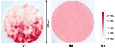
Figure 3. (a and b) Pressure distribution across a 100-mm-diameter imprint field when a 1.38 MPa nominal pressure is applied using SPP and ACP, respectively. (c) Pressure vs color intensity calibration chart.
In contrast, in ACP, when the same nominal pressure of 1.38 MPa (200 psi) is supplied by a gas, the pressuresensitive film exhibits a uniform color across the entire nanoimprint field (Figure 3b), indicating a uniform imprint pressure and complete immunity to the problems suffered by SPP.
Effects of Backside Dust. To further study the effects of dust or topology on the backside of the mold or substrate on imprint pressure uniformity, we place a piece of “large artificial dust”, made of paper of 2.6 x 2.6 cm2 area and 0.1 mm thickness, on the backside of the mold. We then apply a 1.38 MPa nominal pressure using both SPP and ACP methods (Figure 4a and b). Clearly, in SPP (Figure 4c) under the backside-dust conditions, all of the applied force is concentrated under the “large artificial dust”, with a pressure reading well exceeding 2.5 MPa (the upper bound of the measurement range of the pressure-sensitive film), whereas the area surrounding the dust area has almost no imprint pressure (the pressure is below the 0.5 MPa lower bound of the pressure-sensitive film). In contrast, in ACP (Figure 4d) under the same condition, the “large artificial dust” has no effects on the imprint pressure, which remains uniform across the entire 100-mm-diameter imprint field.
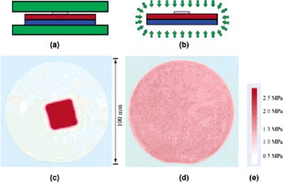
Figure 4. (a and b) Schematics of experimental setups for studying the effects of backside dust/topology in SPP and ACP, respectively. (c and d) Pressure distributions across a 100-mm-diameter imprint field when a paper piece of 2.6 x 2.6 cm2 in area and 0.1 mm in height is inserted on the backside of the mold, and a 1.38 MPa nominal pressure is applied using SPP and ACP, respectively. (e) Pressure vs color intensity calibration chart.
Effects of Dust Trapped Between Mold and Substrate. To study the effects of the dust trapped between the mold and the substrate on pressure distribution in both SPP and ACP, we place a “small artificial dust particle”, which is a triangularly shaped paper piece with an in-plane dimension of 1 mm and height of 0.1 mm, between the mold and the pressure-sensitive film. Again, the same nominal pressure of 1.38 MPa is applied in the two different pressing methods (Figure 5a and 5b). In Figure 5c, in SPP under this trappeddust condition, the dust has a global effect on the pressure distribution across the entire 100-mm-diameter imprint field, causing distinct variations in pressure and contact. More than 60% of the imprint field around the dust site shows poor contact and a pressure below 0.5 MPa, whereas an extremely high pressure is applied on the dust site. In contrast, in ACP under the same condition, the effects of dust on the pressure distribution are localized to a small area (Figure 5d). The affected area is limited to a circle 6 mm in radius, due to local wafer deformation. The pressure distribution outside this circle remains uniform.
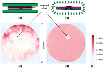
Figure 5. (a and b) Schematics of experimental setups for studying the effects of trapped dust in SPP and ACP, respectively. (c and d) Pressure distributions across a 100-mm-diameter imprint field when 0.1-mm-high paper dust is trapped and a 1.38 MPa nominal pressure is applied using SPP and ACP, respectively. (e) Pressure vs color intensity calibration chart.
The exact radius of the affected area depends on the applied gas pressure and the effective dust particle height under pressure and in-plane dimensions. For a dust particle of a spherical shape and an effective particle height of h (tens of micrometers or more), the radius of affected area can be estimated using analytical solution based on classical plate theory13
where p is the applied gas pressure, t, E, and i are t
he thickness, elastic modulus, and Poisson’s ratio of the wafers, respectively, assuming that the mold and substrate are wafers of identical mechanical and geometrical properties, and no pressure-sensitive films are inserted (which is true for real imprint processes). This solution is valid for large r/t ratios. For more complicated situations, numerical solutions may be obtained using finite element modeling.14
Moreover, the effects of real dust on the imprint by SPP and ACP are studied. The dust particles of heights of ~10 μm and in-plane diameters of around 0.1 mm are placed between the mold and substrate. We carry out a thermal NIL process at 120°C, and a nominal pressure of 1.38 MPa (200 psi) using both SPP and ACP, with a mold of 200 nm period gratings (made by interference lithography) on a 100-mmdiameter silicon wafer, imprinted to a 180-nm-thick Nanonex NXR-1040 thermoplastic polymer resist film spin-coated on a 100-mm-diameter single-side polished silicon substrate that is 0.5 mm thick. The results are shown in Figure 6. The red arrows point to dust particle sites. In SPP (photograph in Figure 6a), the affected areas of two dust particles 5 mm away overlap and form an elongated defect area 18 mm in length in which no grating patterns are imprinted. In contrast, in ACP (optical micrograph in Figure 6b), the affected areas of two dust particles 3 mm away are isolated, and each forms a circle 0.5 mm in radius, which is over a factor of 10 smaller. The SEM image in Figure 6c shows the resist as imprinted in ACP and is taken 0.8 mm from the center of one dust particle. The imprinted gratings outside the circle are not affected by the dust. This shows great ability of ACP to minimize dust effects and improve yield.
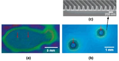
Figure 6. (a) Photograph of dust affected area in SPP. (b) Optical micrograph of dust-affected area in ACP. (c) SEM image of imprinted 200 nm period gratings in resist 0.8 mm from a dust center in ACP. Red arrows in parts a and b point to dust sites.
Effects on Thermal Imprint Speed. Finally, we investigate the ACP’s advantage of small thermal mass for fast thermal imprint by carrying out a full wafer (100 mm diameter) thermal nanoimprint using NX-1000. A silicon mold of 200 nm period gratings covering the full 100-mmdiameter area was used to imprint a 180-nm-thick Nanonex NXR-1040 thermoplastic resist film on a 100-mm-diameter silicon wafer. The process is carried out at 120°C and 1.38 MPa (200 psi) with the temperature and pressure recorded in real time, and radiative heating and convection cooling are used. As shown in Figure 7, the heating and cooling take only 5 and 8 s to and from 120°C, respectively. The whole process including evacuating the chamber takes 57 s to complete. The imprint quality is examined by taking topview SEM images at five different locations, one at the center of the wafer and four others on a circle 1 cm from the wafer edge, as shown in Figure 8. The five-point SEM shows great pattern uniformity over the full wafer imprint field by the fast thermal imprint using ACP.
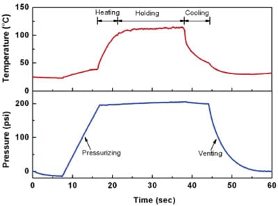
Figure 7. Temperature and pressure recorded during a thermal nanoimprint process using ACP. The short sub-60-s imprint time is attributed to the small thermal mass in ACP.
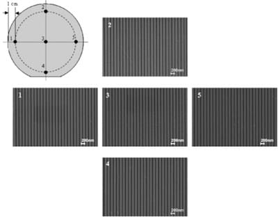
Figure 8. Top-view SEM images taken from five locations on the 100-mm-diameter sample imprinted by the sub-60-s thermal NIL, one at the center and four on a circle 10 mm from the wafer edge. Each SEM is labeled with a number from 1 to 5, corresponding to the location from which it is taken. Uniform 200 nm period gratings are observed at all locations.
In summary, we have studied and compared the pressure distribution, yield, and imprint speed over a 100-mmdiameter nanoimprint field for two different pressing methods, solid parallel plate press (SPP) and air cushion press (ACP). Pressure nonuniformity in SPP is investigated and the pressure variation across the imprint field is measured to be more than a factor of 5. Ultra-uniform pressure distribution is demonstrated for ACP. In addition, ACP is fully immune from any backside dust or topology of the mold and substrate and localizes the effects of trapped dust, all of which severely disrupt the pressure distribution in SPP. Using ACP, we have further demonstrated thermal imprinting with excellent uniformity and high yield over a 100 mm imprint field in less than 60 s.
Acknowledgment. This work was supported in part by DARPA.
REFERENCES
1. Chou, S. Y.; Krauss, P. R.; Renstrom, P. J. Appl. Phys. Lett. 1995, 67, 3114.
2. Chou, S. Y.; Krauss, P. R.; Renstrom, P. J. Science 1996, 272, 85.
3. Austin, M. D.; Ge, H.; Wu, W.; Li, M.; Yu, Z.; Wasserman, D.; Lyon S. A.; Chou, S. Y. Appl. Phys. Lett. 2004, 84, 5299.
4. Austin, M. D.; Zhang, W.; Ge, H.; Wasserman, D.; Lyon, S. A.; Chou, S. Y. Nanotechnology 2005, 16, 1058.
5. Li, M.; Chen, L.; Zhang, W.; Chou, S. Y. Nanotechnology 2003, 14, 33.
6. Macintyre, D. S.; Chen, Y.; Lim, D.; Thoms, S. J. Vac. Sci. Technol., B 2001, 19, 2797.
7. Cao, H.; Yu, Z.; Wang J.; Chou, S. Y. Appl. Phys. Lett. 2002, 81, 174.
8. Li, M.; Chen, L.; Chou, S. Y. Appl. Phys. Lett. 2001, 78, 3322.
9. https://public.itrs.net.
10. Zhang, W.; Chou, S. Y. Appl. Phys. Lett. 2001, 79, 845.
11. Chou, S. Y.; Zhuang, L. J. Vac. Sci. Technol., B 1999, 17, 3197.
12. Chou, S. Y. U.S. Patent 6,482,742.
13. Timoshenko, S.; Woinowsky-Krieger, S. Theory of Plates and Shells, 2nd ed; McGraw-Hill, New York, 1959.
14. Tejeda, R.; Engelstad, R.; Lovell, E. J. Vac. Sci. Technol., B 2002, 20, 2940.


