Björn Backlund, Toni Schweizer – ABB Switzerland Ltd
Introduction
Press-pack high power semiconductors are in many applications very powerful components in controlling electrical power. To utilise their full potential a proper mechanical design of the complete assembly, including press-pack high power semiconductors, heat sinks, bus bars and other components, is crucial. In this application note some important issues for the mechanical design and the assembly work for stacks using press-pack high power semiconductors are addressed.
2 – Recommendations for the interface properties
The current and heat conducting interfaces should be designed to retain good conduction properties throughout the equipment lifetime. This is accomplished by creating a sufficient number of stable metal-tometal connections, referred to as “a-spots” in contact theory, which can efficiently conduct current from the semiconductor through the heat sink to the bus bars. These a-spots must be maintained during hard stress conditions such as load cycling, vibration and chemical contamination such as sulphur gases. To achieve this, care must be taken in choosing the right materials for the components. They must be coated properly and have the right surface finish. In this application note we concentrate on the interface between the presspack high power semiconductor and the heat sink.
2.1 Definitions
Roughness: The surface roughness is a measure of the microstructure of the surface. It is expressed as an Ra-value as per ISO 4287. The roughness is Ra ≤ 0.8 µm for all ABB Switzerland Ltd, Semiconductors (ABB) semiconductor press-pack devices.
Flatness: The flatness is ≤ 10 µm for ABB devices with pole piece diameter ≤ 50 mm and ≤ 15 µm for ABB devices with pole piece diameter > 50 mm. This means that a specific pole piece surface is limited by two parallel planes at a maximum distance of 10 or 15 µm apart.
FM: The mounting force is the recommended force to be applied for optimal device performance. The data sheet limits are not guaranteed at too low a mounting force. The thermal impedance and the on-state voltage drop will increase, and the surge current rating will decrease when the force is reduced below the rated value. Too high a mounting force may reduce the load cycling capability by excessive deformations of the fine wafer structures or, at worst, by silicon wafer cracks.
2.2 Design of the utilised components
When using water-cooled heat-sinks the cooling should be as homogeneous as possible over the entire contact surface of the device. A single water channel through the centre of the heat-sink may not be sufficient for heavy-duty equipment and could lead to over heating of the device rim. It is advisable to use water channels that create turbulences rather than using simple straight paths (though this may be sufficient for light duty units). ABB supplies compact water-cooled heat-sinks for heavy-duty equipment see Figure 1. These heat-sinks use a stainless steel spiral tube on both sides of the surface to optimise cooling. For more information about heat sinks see the contacts in section 4.2.
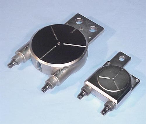
Figure 1 Water-cooled heat-sinks supplied by ABB
The heat-sinks must have adequate mechanical robustness to withstand compression with forces up to 135 kN without deformation. Deformation could lead to inhomogeneous pressure distribution.
Cast or extruded heat sinks need, in almost all cases, to be machined properly through processes such as milling or fine turning to get to the recommended surface finish.
2.3 Surface treatment
Surface finish and treatment are crucial for optimal heat and current conduction over the device and heat sink interface. The press-pack high power semiconductors from ABB have a maximum surface roughness of Ra = 0.8 µm and flatness below 10 or 15 µm depending on pole piece size. It is recommended that the heat-sink surfaces have the same flatness and roughness as the press-pack high power semiconductor measured on the surface where the device is to be mounted.
ABB recommends the use of heat sinks with a good quality plating of nickel or silver. For applications with hard component stress, ABB recommends chemical plating rather then electrolytic plating. Bare copper or aluminium is not recommended due to corrosion that rapidly deteriorates the contact surfaces. Nickel and silver do corrode, however nickel and silver oxide do not deteriorate the interface to the same extent as aluminium oxide. The ABB press-pack high power semiconductors have pole pieces of copper with a nickelplating of approximately 5 µm. When using nickel-plating it is recommended to use the same plating thickness on the heat-sink area that is in contact with the device.
A thin film of a light grease or special silicone oil may be applied on the contact surfaces before the devices are assembled between the heat sinks. The interface grease or silicone oil must be carefully chosen for its long-term chemical stability, corrosion inhibiting properties, temperature range, electrical properties and ease of use. ABB recommends Silicone oil type SF1154 (GE) supplied by ABB Automation Technologies, see paragraph 4.2 for contact information.
The recommendations for the heat-sinks are also valid for all other components used in contact with the press-pack semiconductor such as the bus bar connecting the non-cooled side of the press-pack semiconductor in single side cooled assemblies.
3 – Recommendations for the mechanical design and assembly
The mechanical design and the assembly of the stack are also crucial for the performance and reliability of the press-pack high power semiconductor. Inhomogeneous pressure distribution caused by the mechanics is a common cause of device failure. In this section we cover some important issues in designing reliable stacks.
3.1 The mechanical design
The clamping must be carefully designed to ensure that the device is clamped with the right force and it must also allow homogeneous pressure distribution over the whole contact surface of the device. Uneven pressure will lead to deformation of the housing and internal stress between the different layers inside the device causing it to fail prematurely during load cycling. Designing for pressure uniformity is not always easy and the complexity should not be underestimated. Simple solutions, such as clamping the device bet
ween two rectangular plates by bolting down the corners will exhibit poor reliability. To verify that the pressure distribution is uniform, ABB recommends the use of Fuji Prescale film or similar products. For information about the Fuji Prescale film see www.fujiprescaleusa.com. Most devices are measured using the Fuji Prescale film medium pressure grade, 1 – 5 kN/cm2, but some devices, mainly large area GTO and IGCT, are measured using low-pressure grade, 0.25 – 1 kN/cm2. Figures 2 and 3 show two samples from pressure distribution measurements on IGCT’s with the Fuji Prescale film. Figure 2 shows good pressure distribution and figure 3 poor pressure distribution with a large area of the device having too low a pressure and some areas having to high a pressure.


Ideally, the mounting force should be applied from a single point above the centre of the device. Our recommendation is that the centre of the force is within 2 mm from the centre of the device, and at a minimum distance equal to half the pole-piece diameter of the device from the device surface, as shown in Figure 4. This to achieve good pressure uniformity considering the “90 ° force cone”. A spherical cup between the mounting clamp and the pressure spreader above the heat-sink can act as this single point of force and ensures that the force from the mounting clamp is transferred symmetrically to the device. It also allows parts within the stack to adapt to inherently present non-parallelisms. There will always be inherent nonparallelisms in a stack since it is not possible to manufacture heat sinks and press-pack high power semiconductors with perfectly parallel surfaces. Therefore, non-parallelisms should be reduced as much as possible. The non-parallelism between the anode and cathode pole pieces is ≤ 100 µm for ABB devices with pole piece diameter ≤ 50 mm and ≤ 150 µm for ABB devices with pole piece diameter > 50 mm.
Due to space restrictions in some applications, it may not always be practical to use the recommended half pole-piece diameter of distance, but reasonable results can also be obtained with smaller distances when stiff materials such as steel are used for the force spreader, possibly together with Belleville springs.
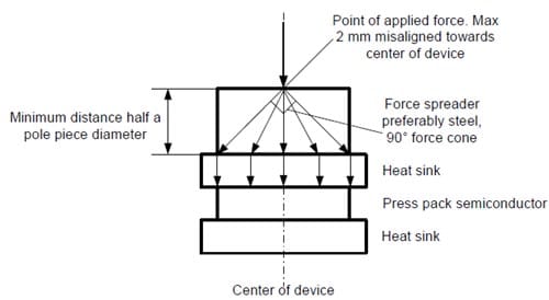
Figure 4 Recommended application of the mounting force.
ABB sells a series of mounting clamps for mounting forces 4 – 135 kN. For further information please contact ABB Automation Technologies, see paragraph 4.2 for contact information. An example of a 135 kN clamp can be seen in the left stack of Figure 5.
The components and the clamp design must be chosen to withstand temperature levels and forces caused by mechanical expansions and contractions, due to temperature changes that occur during working conditions, without damage. This over the whole equipment lifetime. The design must also allow for temperature expansion and contraction without large changes in force and pressure distribution on the presspack high power semiconductor.
In long stacks with more than 2 devices and their heat sinks, it may be difficult to obtain good mechanical stability when using a design with 2 rods and a standard mounting clamp. Therefore ABB recommends the use of a 4-rod Belleville spring construction for long stacks as shown in Figure 5.
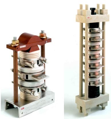
Figure 5 Two rods are enough for shorter stacks, but for longer stacks 4 rods are recommended.
Press-pack high power semiconductors, whether parallel or anti-parallel connected, should always be clamped separately as shown in Figure 6, unless they are stacked as shown in Figure 5. Due to mechanical tolerances there will be differences in height and parallelism that in many cases will create mechanical forces large enough to significantly reduce the lifetime of or even destroy the devices if 2 or more devices are clamped together between two rigid bus bars or heat sinks.
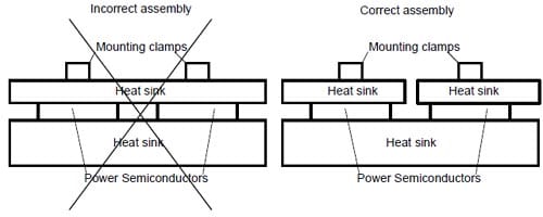
Figure 6 Devices should be individually clamped.
If the mounting clamp and the bolts have to be on ground potential, the right materials and the right air and creepage distances must be utilised. For more details about insulation co-ordination consult standards IEC 60664-1 and UL840. Insulating materials, as Vetresit®, a glass-fibre epoxy from ABB, can be used for the bolts allowing for a simplified or more compact stack compared with steel bolts, that either requires insulation or need enough air strike distance between the live parts.
If several devices are assembled together in one stack with the same mounting clamp, the devices must have the same rated mounting force. This is to avoid over-stress or too low a pressure for some of the devices in the stack. It is also advisable to use devices with the same pole piece diameter to simplify the heat-sink design in order to achieve good pressure distribution on all devices. If the heat sink cannot spread the pressure evenly and devices with different pole piece diameters are used, there is a high risk that either the rim of the smaller device gets too high a pressure or the rim of the large device gets too low a pressure. An example of a well-dimensioned stack is shown in Figure 7. Figure 8 shows a badly designed stack using only thin force spreaders and insufficient heat sinks that do not spread the force evenly over devices with different diameters. ABB does not recommend this, but with well-designed heat sinks and force spreader assemblies, as shown in Figure 8, can be designed.
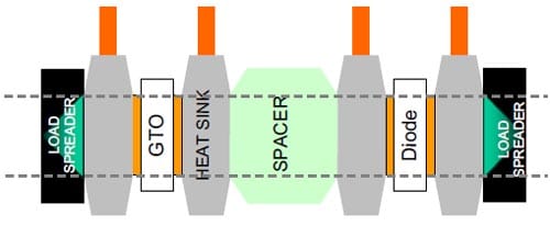
Figure 7 Well designed stack with effective load spreaders and similar device diameters.
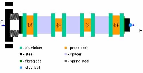
Figure 8 Poorly designed stack with ineffectual load spreaders and dissimilar device diameters.
Bus bars or their connections to the stack should have a flexible part to avoid mechanical stress to the stack assembly. Mechanical stress can occur either due to mechanical tolerances or due to heat expansion and contraction during changes in the electrical load.
For IGCT-assemblies an additional issue is that the integrated gate drive needs a fixture in order to withstand vibration stress applied during stationary operation and transportation. Note that the gate unit, and in the case of large devices, also the metal casing around the gate unit, are on cathode potential and need to be insulated from the rest of the assembly.
The gate cables for PCT and GTO should be laid properly to ensure that they do not come in contact with anode potential and also to minimise electro-magnetic disturbances. Twisted or coax cables are recommended to reduce EMC sensitivity. The cables should be as short as possible and they should preferably be laid in a 90 ° angle to the main current conduction direction.
For water-cooled assemblies very stiff tubes used between the different heat sinks can cause problems. This is due to mechanical forces caused by thermal expansion and contraction. Since water is electrically conducting the tube length between heat sinks with different potential
must be long enough. De-ionised water should be used together with water treatment equipment needed to remove conducting particles and to keep the water conductivity low. ABB recommends the use of non-corroding material such as stainless steel and Teflon for water tubes, not copper or aluminium.
For equipment used at severe environmental conditions special care must be taken to ensure that the presspack high power semiconductors are not harmed by vibrations, temperature variations, etc. Special care regarding vibrations must be taken in applications for rolling stock.
3.2 Example of a GTO fixture
In Figure 9 an example of a GTO -stack is shown with a short reference to some of the issues mentioned in section 3.1.
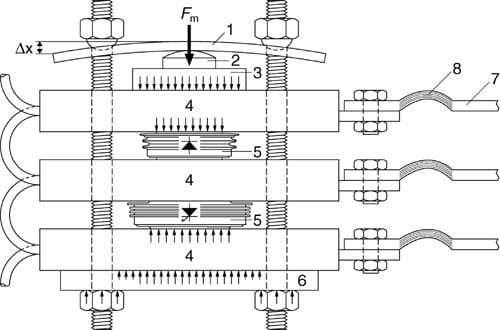
Figure 9 Example of a stack, illustrating the basic rules for correct clamping of press-pack high power semiconductors
- Leaf spring. Spring excursion Dx must be large in comparison with thermal expansion of stack parts in order to keep FM constant over time and temperature variations.
- Spherical cup ensures that Fm is transferred symmetrically to the press-pack high power semiconductors and allows the parts within the stack to adapt to inherently present nonparallelisms.
- Strong steel plate for homogeneous pressure transfer to heat-sink (4), symbolised by small arrows.
- High-quality heat sink: Clean and parallel surfaces with flatness and roughness as per paragraph 2.3.
- Press-pack semiconductor: Surfaces cleaned and covered with thin film of silicone oil before mounting.
- Strong yoke ensures homogeneous pressure distribution on heat-sink (4), symbolised by small arrows.
- Bus bars (7) connected to heat-sinks (4) by means of flexible connections (8) to avoid uncontrolled “external” forces disturbing homogeneous pressure distribution within the stack.
- Before mounting the stack parts in the clamping system, the various surfaces should be cleaned with alcohol, ethanol or similar, and it may be advantageous to lubricate them with a thin film of silicone oil to improve the thermal contact, and to prevent corrosion if the stack is exposed to an aggressive environment. However, it should be noted that silicone oil or contact grease will never compensate for poor quality heat-sink surfaces!
3.3 Example of an IGCT fixture
Under conditions of severe vibration, IGCT gate units cannot be stabilised solely by the GCT clamped to its heat sinks. The gate units have 2 pairs of M4 holes, one M4 pair between GCT housing and gate-unit housing, which can be used for a heat-sink fixture and one M4 pair on the rear edge of the housing. The outline drawing in Fig. 10 shows the location of these M4 holes. The length of the screws must be chosen to ensure that they do not penetrate more than 10 mm into the thread.
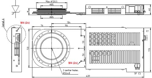
Figure 10 Outline drawing of 5SHY 35L4510 with M4 holes for mechanical fixture of gate unit part.
In Fig. 11, a simple stack design for vibration testing is shown. Only the M4 pair on the rear edge of the housing was used in this test which was used to establish conformance with ABB specification 5SZK9107-00 (“Specification of environmental class for pressure-contact IGCTs – Operation”).
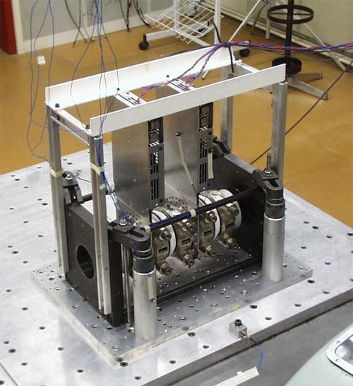
Figure 11 Stack assembly for vibration testing of 5SHY 35L4510.
3.4 Recommendations for assembly
Even the best of designs will not lead to the intended result if the stack is not assembled correctly. In this section some issues of importance for the assembly work are described.
If necessary the surfaces of the heat sinks and semiconductors should first be lightly polished with 3M ScotchbriteTM or a similar product. Before assembly, the contact surfaces must be thoroughly cleaned using ethanol (or similar solvent) and a lint-free cloth. The assembly should be carried out in a clean environment free of dust and humidity as the surfaces must be kept clean during the whole assembly procedure. Heat-sink and semiconductor surfaces should not be touched with bare hands. We recommend the use of lint-free gloves for the handling of semiconductor devices and heat-sinks.
The heat-sinks and press-packs should be handled with care to avoid scratches and other damages to the surfaces. Small scratches should be avoided (even though they are not detrimental to contact integrity since it is the overall surface finish which determines contact quality). The surface finish must remain within the specification given earlier and the plating should be intact to avoid subsequent corrosion of the underlying metal.
Silicone oil should be applied sparingly and spread uniformly.
Ensure that the devices are placed with the right polarity, that the gate cables for thyristors and GTOs are placed correctly and make sure that the devices are well centered and fixed. The centering is normally done either through a holder gripping the pole pieces or the ceramic or through a central pin fitting into the centering hole of the device.
At the start of clamping, the mounting force indicator must be set to zero and the clamp suppliers assembly instructions followed carefully.
Press-pack high power semiconductors should be fully clamped prior to attaching bus bars to the assembly. This will avoid misalignment of the press-pack high power semiconductors during assembly.
4 – Additional notes
4.1 – Further things to consider
Unless the press-pack high power semiconductors and heat sinks are mechanically well supported, long stacks with several devices should be transported in the upright position. Having the stack in its horizontal position can cause tension to the press-pack high power semiconductors with consequent damage, and vibrations or bumps may lead to device destruction.
When designing a stack, the stack installation in a cubicle or at site should be taken into consideration, in order to simplify the installation in the cubicle and to ensure that the external connections fit. If using conductive material in the clamp, include connection points for grounding of the stack. Heavy stacks should have hooks or other support for handling purposes. For air-cooled units, both convection and forced air, adequate airflow must be assured and pressure drops and additional heating in the cubicle must be considered in the thermal design of the unit.
4.2 Application support for assemblies
For further information please to contact:
Application engineering:
Björn Backlund
Tel: +41 58/5861 330
Fax: +41 58/5861 306
E-Mail: [email protected]
Water-cooled heat sinks and stack construction:
Adriaan Welleman
Tel +41 58/5861 894
Fax: +41 58/5861 310
E-Mail: [email protected]
Mounting clamps, heat sinks and cleaning tools:
ABB Automation Technologies
Logistics Center, Semiconductors
SE- 721 59 Västerås
Sweden
Tel: +46 21/322912
Fax +46 21/322977
E-Mail: [email protected]
ABB Switzerland Ltd
Semiconductors
Fabrikstrasse 3
CH-5600 Lenzbur
g
Switzerland
Tel: +41 58/5861 419
Fax: +41 58/5861 306
E-Mail: [email protected]
Internet: www.abb.com/semiconductors


