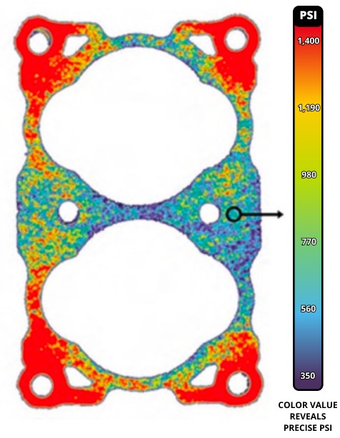
Pressure Measurement Film is an affordable and easy to use tool that reveals the distribution and magnitude of pressure between any two contacting, mating, or impacting surfaces. It is a Mylar®-based film that contains a layer of tiny microcapsules. The application of force upon the pressure measurement film causes the microcapsules to rupture, producing an instantaneous and permanent, high-resolution image of pressure variation across the contact area.
Pressure measurement film is extremely thin (4 to 8 mils), which enables it to conform to curved surfaces. It is ideal for tight spaces not accessible to conventional electronic transducers. Simply place the film between any two surfaces. Then, apply and remove pressure. Immediately, the pressure measurement film reveals the pressure distribution profile that occurred between the two surfaces. Like Litmus paper, the color intensity of the film is directly related to the amount of pressure applied to it. The greater the pressure, the more intense the color.
He Gao, Hua Tan, Wei Zhang, Keith Morton, and Stephen Y. Chou of the Nanostructure Laboratory at Princeton University used pressure measurement film to evaluate manufacturing methods for nanoprint lithography, a process that creates patterns for integrated circuit (IC) components. This work was titled, “Air Cushion Press for Excellent Uniformity, High Yield, and Fast Nanoimprint Across a 100 mm Field”. It was published in Nano Letters, 2006, Vol 6, No 11, pp 2438–2441. Fujifilm Prescale® pressure measurement film was used exclusively for this study.
The pressure uniformity of a Solid Parallel-Plate Press (SPP) was compared to that of an Air Cushion Press (ACP) during the manufacturing process for ICs. Figure 1 shows simplified schematics of the two presses.
| Fig 1a: Schematic of a Solid Parallel-Plate Press | Fig 1b: Schematic of an Air Cushion Press |
To investigate the pressure distribution of SPP and ACP over an imprint field of 100 mm diameter, pressure measurement film was placed between the mold and substrate, both of which were 100-mm-diameter prime silicon wafers of 0.5-mm thickness with flat featureless front surfaces and unpolished backsides. Figure 2 shows the results when a nominal pressure of 1.38 MPa (200 psi) was applied.
The Fujifilm Prescale® pressure measurement film shows that the pressure in the SPP varies tremendously across the wafer (isolated local domains with strong and light colors). Also, the lower half of the SPP image has a much higher average pressure than the upper half due to nonparallelism between the two pressing plates. In contrast, the ACP image exhibits a uniform color across the entire nanoimprint field.
 | |
| Fig 2a: Pressure Distribution on SPP | Fig 2b: Pressure Distribution for ACP |
The effects of backside dust and dust trapped between the mold and substrate are illustrated in Figures 3 and 4.
| Fig 3: Backside Dust Effects, (a) & (c) SPP, (b) & (d) ACP, (e) Pressure vs Color Intensity | Fig 4: Trapped Dust Effects, (a) & (c) SPP, (b) & (d) ACP, (e) Pressure vs Color Intensity |
As a result of the images obtained with the Fujifilm Prescale® pressure measurement film, He Gao, et al, concluded that the air cushion press was preferred over the solid parallel-plate press. For ACP, pressure distribution was more uniform. Furthermore, ACP was immune from any backside dust or topology of the mold and substrate. ACP also localized the effects of trapped dust.


