Article: Wafer & Device Packaging and Interconnect
Wafer-to-wafer bonding has become an enabling semi-conductor technology in industries such as 3D packaging, MEMS, MOEMS and SOI. In a typical wafer bonding process, two flat substrates are permanently joined (bonded) to one another by applying physical pressure, temperature and/or an electric field (Figure 1). Each of these parameters is set depending on the substrate materials being bonded, and controlling these parameters is crucial to a successful, high-quality, high-uniformity manufacturing process.
Of these three major parameters, electric field and temperature are readily measurable within a wafer bonding chamber using built-in electronics and thermocouples. However, pressure is usually measured in the tool as the total amount offeree exerted over the pressure column. This measured force is then used to calculate the average pressure, assuming perfectly flat pressure plates. However, in practice, the pressure plates are often non-ideal, or they may have degraded over time. This leads to potential pressure variations that are not detected by the control software. Poor distribution of pressure can lead to poorly bonded or completely unbonded wafer areas, cracked wafers, or premature wear of the pressure plates.
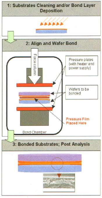
Figure 1. Wafer Bonding precess.
The significance of a uniform applied pressure in a bonding process depends largely on the specific materials being bonded. For example, in an anodic bonding process, silicon is bonded to glass by applying a large electric field (500V) at elevated temperatures (> 300°C).¹ The reaction between silicon and oxygen then forms a very strong SiO2 bond. Because the magnitude of the electrostatic forces is generally sufficient for a full bond, physical applied pressure is neither critical nor required for this type of bond process.
However, the control of applied pressure is important in eutectic or thermocompression bonding processes, where two arbitrary substrates are bonded together using thin intermediate films that are often metallic alloys.1-3 In this type of bond, the two surfaces to be bonded are brought into contact and the temperature is increased to above the eutectic point. Once the eutectic temperature is reached, the solder liquefies and the wafers bond if they are in contact.
High pressure can cause the liquefied solder to physically compress and potentially spread onto unwanted regions and cause short circuits. Too little pressure typically results in weakly bonded or completely unbonded regions. And in practice, for a non-optimized bonding system (considering bond process parameters as well as materials used), both spill-outs and ubonded regions can be found on the same pair of substrates due to pressure, temperature or solder non-uniformities. Therefore, the characterization of applied pressure measured directly at the substrate is important in the development of high yielding bond processes.
Pressure Indicating Film Experiment
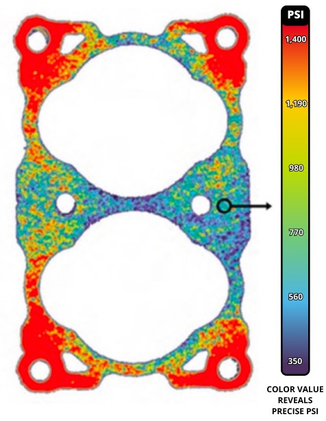
Pressurex® film is a pressure sensitive film that measures pressure from 2 to 43,200 psi (0.14 – 3,000 kg/cm² ). When placed between contacting surfaces, it permanently changes color proportionally with the pressure applied. Absolute pressure magnitudes were calibrated using known pressures, which were then used to analyse scanned pressure maps and create colored pressure maps such as that shown in Figure 2b.
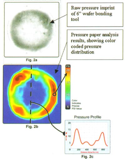
By running a bond recipe with the pressure set to 4 bar, a direct imprint is formed on an appropriate grade of pressure film. Figure 2a shows an image film taken from a 6-inch diameter bonding tool with poor pressure uniformity. The color map in Figure 2b emphasizes the donut shaped high pressure ring. The line scan in Figure 2c shows outer ring pressures exceeding 15 bar and less than 3 bar at the center.
A series of adjustments to the pressure column of the bond tool were then made, and the pressure uniformity was evaluated by running the same bond recipe on the same range pressure film. The images in Figure 3 show the adjustments resulting in improved pressure uniformity. Note that after the adjustments, the pressure film analysis shows an offset from the intended recipe pressure of 4 bar, which is a by-product of the instrument assuming a particular wafer area.

In addition to troubleshooting the pressure distribution, the same pressure film data can be used to monitor and maintain performance in manufacturing practices, such as six-sigma statistical process monitoring.
Au/Sn Eutectic Wafer-to-Wafer Bond
Improvements in wafer bond pressure uniformity were applied to a specific project requiring both reliable inter-wafer electrical connections (~103-104 per wafer), wafer-to-wafer separation of 2-3 µm, excellent bond gap control, high bond strength and a liquid-proof sealing. Liquid-proof sealing was required for further processing of the bonded stack through metal deposition, lithography and etching steps.
Besides these main requirements, the bonding process should not create large stresses that would cause MEMS device performance degradation or reliability issues due to stress relaxation over time. Sources of stress can be the bonding process itself or mismatch of the bonding material thermal expansion coefficients. Preferably, the same process can be used for bonding a third wafer to the stack of two bonded wafers.
Au/Sn Eutectic Wafer-to-Wafer Bond Steup
Our experiments used electroplated Au/Sn solder, aiming for an 80% Au and 20% Sn composition and eutectic temperature of 278°C.² Control of the exact solder composition is critical, be- cause a small variation in composition in either direction increases the melting temperature significantly.
For example, a +3% shift in composition results in a melting temperature of 340°C; and on the other side, a -3% shift results in 333°C melting temperature. Because the solder thickness is comparable to the seed metal thickness, the amount of Au in the seed metal is also critical.
The upper and lower wafers bonded in this device are: MEMS wafers containing micromachined devices with a ring of seed metal around each die; and CAP wafers containing a corresponding solder ring with underlying seed metal. The solder should wet to both wafers during bonding, thus providing a mechanical bond and a hermetic seal.
For initial analysis and test purposes, the silicon MEMS wafers were replaced with glass bond test wafers. SiO2 standoff features in the CAP wafers were included to provide a mechanical stop so that when solder compresses during bonding, the final gap between the substrates is well determined (Figure 4).
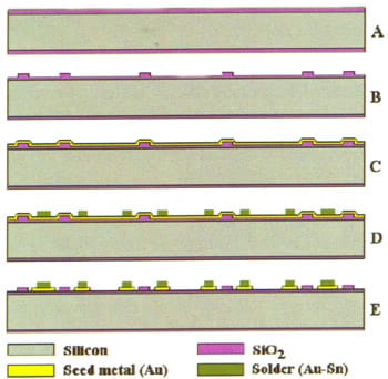
Fabrication of the CAP wafers is shown schematically in Figure 4. Standard thickness 6-inch wafers with TTV smaller than 5 µm were used. After initial oxidation (A), standoffs were defined by oxide patterning. Caps re-oxidation followed (B). Typically, initial oxide thickness was 3.1 µm and 1.0 µm thick oxide was grown at the second oxidation step; the resulting standoff height was 2.6 µm. Seed metal (4000 A Au) was deposited on the Caps (C) and Au/Sn solder was plated using a photoresist mask (D).
Initial plating tests were made using an R&D setup, while later work was done using an industrial-grade Cup plater. Plated solder was typically 65% Au and 35% Sn, 2.0-2.5 µm thick, with 5-10% non-uniformity across the wafer. Patterning and removal of the seed metal layer from non-plated areas was the last step in the pre-processing of Caps (E).
It was also found that the design of the seed metal pattern has an affect on the bond results.³ Patterns of several thin solder lines (50-60 µm wide) provided better sealing than a single, wide solder line of equivalent solder volume. By design, the entire seed layer (4000 A) could be consumed during the bond process to create the eutectic composition. As liquid solder is compressed during the bonding process, additional Au is consumed as the solder floods fresh areas of the patterned seed layer.
Although the Au diffusion in the solder is fast, the Au concentration at the periphery of the solder line can be greater than the concentration at the center of the solder line. This difference in composition can make the solder difficult to compress. It was found that several line lines of solder yielded the most consistent results.
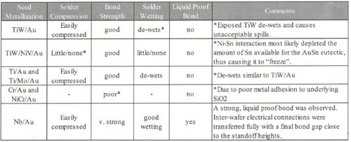
The bonding process was done in a wafer bonder under vacuum with a bond temperature between 300°C and 350°C. The applied pressure was set at 4 bar and, in most cases, using the corrected pressure plates mentioned previously. Several types of seed metal were studied, with results summarized in Table 1. For all tests shown here, glass bond test wafers were used instead of the silicon MEMS wafers to allow visual evaluation of solder flow.
Experiment Results on Seed Metallization
For TiW/Au, Ti/Au and Ti/Mo/Au, the common problem was solder spill-out after de-wetting of the solder from the seed metallization. Figure 5 shows an example of spill-outs in this circumstance. Figure 6 shows a wafer-level photograph of spill-outs using TiW/Au. For wafers with de-wetting solder, the resulting bond was reasonably strong mechanically (in most cases strong enough to survive dicing) but not liquid-proof.


The TiW/NiV/Au seed metal is a good example of several difficulties inherent in thin-film solder systems. In this case, the solder did not compress or flow due to the presence of Ni in the seed metal. EDX analysis of the solder-seed interface showed Sn depletion, likely caused by a Ni/Sn interaction. With insufficient Sn available to the Au, solder composition is non-eutectic and frozen all the way to the maximum temperature of 350°C. Because the solder was not liquefied, there was minimal solder flow and little or no compression. Surprisingly, the resulting bond still had good mechanical strength.
The best results were achieved with Nb/Au seed metallization.3,4 Here the solder is liquefied, the gap easily compressed to bond strength was good and provided liquid-proof sealing of the dies. The final bond gap between the wafers was at the desired standoff height.
Figure 6 is a photograph of an example half-wafer bonded using Nb/Au metallization and a half-wafer bonded with TiW/Au metallization. The two samples were bonded separately using the same bond tool and then later broken in half. The de-wetting from the TiW metallization (left side) is clearly visible even with the naked eye.
In Figure 6, the left half-wafer (TiW/Au seed) shows solder spill-out after bonding as caused by de-wetting of solder. Notice that the pressure non-uniformity is evident by observing that the spill-out is most severe on the outer ring of the wafer and much less towards the center. The right half-wafer (Nb/Au seed) is well-bonded, with no solder spill-outs. The pressure non-uniformity is not evident on the right side.
Au-Sn Solder Compression vs. Bond Pressure
The amount of solder compression during bonding directly affects the resulting gap between the bonded substrate surfaces. In this part of the study, the applied pressure was varied from 500 mbar to 4000 mbar, with all else held constant (TiW/Au seed metal was used). The resulting gap was measured at consistent locations across each wafer using a Zygo profilometer and plotted in Figure 7. Each colored set of datapoints represents multiple measurements on a single wafer.
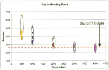
At 500 mbar of applied pressure, the measured gaps are widely spread between 4 µ m to 6.5 µm. At 1000 mbar, the data set showed a general decrease in final gap, which suggests an increase in solder compression. However, the range of data here remained relatively high between 3 µ m and 5.1 µm. As the bond force is increased further to 2000 mbar, the solder continued to compress with increased pressure. Notice that the spread of the data tightened due to the gap approaching the standoff height of 2.6 µm. The gap remained the same as pressure increased from 3000 to 4000 mbar, indicating that the physical stop at 2.6 µm has been reached, and that the standoffs are functioning as expected.
Conclusion
Pressure uniformity in a wafer bonding tool can be effectively characterized using pressure sensitive paper and image analysis techniques. The effect of various types of seed metallization in a Au/Sn eutectic wafer bond were studied. For the range of bond parameters and metals studied, Nb/Au produced the best overall results, offering good mechanical strength, liquid-proof seal and no spill-outs. SiO2 standoffs are an effective way to produce well-defined gaps after bonding.
Acknowledgments
The authors would like to thank Sensor Products Inc. (Madison, NJ, USA) for supplying the pressure paper and the detailed analysis support.
References
- Madou, M. 2002. Fundamentals of Microfabrication: The Science of Miniaturization. CRC Press: Boca Raton, FL. 2nd edition.
- Okamoto, H., and Massalski, T. (editors). 1987. Phase Diagrams of Binary Gold Alloys. ASM International Metals, Park, OH, p. 280.
- Belov, N., et al. 2009. “Thin-Layer Au-Sn Solder Bonding Process for Wafer-Level Packaging, Electrical Interconnections and MEMS Applications.” Pro- ceedings of the International Interconnect Technology Conference, p. 128.
- Chen, H., et al. 1995. “Simple Mb metal bonding structure.” Applied Physic; Letters, 66 (17), p. 2191-4.


