Article: SMT Magazine
by Dr. Thomas Schreier-Alt, FraunhoFer IZM – MMZ, and Jeffrey G. Stark, SenSor ProDuctS, Inc.
IN SUMMARY homogenous pressure distribution within the molding cavity is of particular importance for encapsulation of mechanically-sensitive electronic components, e.g., MEMS sensors, bare dies and flip chips. With the implementation of specially multilayered sensor films, a fast estimation of the pressure distribution within the cavity will be possible.
This article investigates a new pressure measurement method usable during packaging of electronic systems. With pressure-sensitive multilayers, it is possible to determine the pressure distribution on the surface of mold cavities and on various electronic substrates during packaging processes. The pressure sensitive multilayer is based on commerciallyavailable films, such as Pressurex® [1], which change color directly proportional to the amount of pressure applied.
Homogenous pressure distribution within the molding cavity is of particular importance for encapsulation of mechanically-sensitive electronic components, e.g., MEMS sensors, bare dies and flip chips. With the implementation of specially multilayered sensor films, a fast estimation of the pressure distribution within the cavity will be possible. We successfully used the new sensor concept to investigate industrial transfer molding processes with epoxy molding compounds (EMC). On distinct points of the mold cavity conventional piezo pressure sensors have been applied to measure a time-dependent pressure signal.
“With pressure-sensitive multilayers, it is possible to determine the pressure distribution on the surface of mold cavities and on various electronic substrates during packaging processes.”
Introduction
The integration of sensors and actuators transforms classical IC packaging into a complex encapsulation process of multi-chip modules. Reliability of such a mechanically interconnected system in a package is determined by the manufacturing conditions: Process induced pre-stresses interfere with strains during field service; process tolerances have an influence on functionality, reliability and lifetime of the system. The manufacturing process window of a multi-chip module can be much smaller compared to a single-chip encapsulation process and development of a robust production requires improved knowledge of material’s behavior and its interaction with process parameters.
The aspect of thermo-mechanical stress during reactive molding is often neglected, as the encapsulation process itself is considered stress free. Even for epoxies with low viscosity during processing, this assumption is often disproved in practice. The need to monitor forces acting on the embedded electronic parts during the complete polymer encapsulation process is essential considering the spreading usage of MEMS sensors within the automotive industry and their increased demand for signal stability, production tolerances and cost [1]. To meet these demands, microelectronic sensors on chip surface level have been developed [2, 3] providing an accurate insight into the stress distribution. To evaluate the strain distribution within the polymer, optical strain gauges have been adopted by one of the authors [4].
One disadvantage of both active sensors is that the transfer molding process itself can only be monitored if the electrical or optical signals are led through the metal tooling without shorting. To avoid holes or grooves within the tool, Fraunhofer IZM developed a new method to measure cavity pressure based on commercially available pressure indicating films.

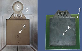
Figure 1: Upper mold tool (left), overmolded PCB substrate with film gate.
Multilayered Pressure-Sensitive Films
This report illustrates, as shown in Figure 1, the optimization of a transfer overmolding process regarding the pressure distribution on a PCB (1) fitted with electronic components (flip chips, quad flat no leads): An epoxy pellet is inserted and compressed by a plunger (2) therefore forced to melt and fill the cavity through the film gate (3). The results of the pressure-indicating film were verified by a Kistler pressure sensor mounted flushing with the mold cavity wall, chronologically recording pressure values at the measurement spot (4).
The piezo sensor from Kistler is sensitive up to pressure values of 2,000 bar/200 MPa. The recorded pressure values during transfer molding of flip chips in the MAP-type package reach up to 130 bar/13 MPa. Figure 2 shows the time-dependent distribution of the pressure recorded at point (4). The maximum pressure is constant for ~10s, afterward a slight pressure increase up to 140 bar is recorded according to the exothermal polymerization process that is heating up the polymer, increasing the pressure within the closed cavity. The polymerization is followed by material shrinkage, decreasing the pressure down to 50 bar. Afterward, the mold tool is opened.
![Figure 2: Typical pressure values [bar] plotted against time [s] recorded by a Kistler pressure sensor.](https://www.sensorprod.com/wp-content/uploads/2023/08/Kistler-line-drawing.jpg)
Figure 2: Typical pressure values [bar] plotted against time [s] recorded by a Kistler pressure sensor.
Disadvantages of pressure sensors within the mold cavity are the missing areal pressure distribution and the occurrence of unattractive marks on the part’s surface, labeled (5) in Figure 1. For most injection-molded parts, these marks are only a decorative defect. For electronic sensors, these marks can result in severe problems during pick and place mounting or laser labeling. To overcome these disadvantages, a multilayer consisting of a pressure-sensing film (sensitivity 100 to 500 bar), an adhesive layer and an isolating polyimide film were mounted on top of the PCB substrate. The isolating film has to fix the pressure film mechanically and prevent it from degassing or swelling (softening temperature of PET resin: 80°C) enabling test durations at 180°C of several minutes without detraction of the sensor function.

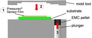
Figure 3: Experimental setup: A PCB substrate is covered on top or bottom
side with a pressuresensitive film. This sandwich is placed between the top and bottom
mold. The epoxy molding compound is injected between the upper pressure film and the top mold.
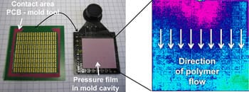
By using a standard molding process, the polymer melt has been injected on top of this multilayer, generating pale red color changes on the pressure indicating film. By digital image recording (scanner) and software processing, the different color intensities of red are transformed into clear distinguishable color values. The digitally-processed film shows a very uniform pressure distribution between 120 and 140 bar (Figure 4). Only at the areas far away from the gate does the pressure drop below 100 bar.

Figure 4: PCB substrate (front side) with removed molding compound
and pressure sensor film. Imaging shows pressure drops with increasing distance to the film gate.
Apart from the pressure within the cavity, the contact area between the upper mold wall and the substrate was analyzed. The first observation is that the film left strong red marks directly on the PCB surface (Figure 4, left). Here the film is squeezed between the PCB substrate and the top mold tool. Frictional movements between the two parts rub parts of the color within the pressure film into the PCB. This effect enabled us to observe directly where the mold tool had contact with the PCB. A uniform and complete contact is necessary to prevent the material from flowing over the substrate (flash).
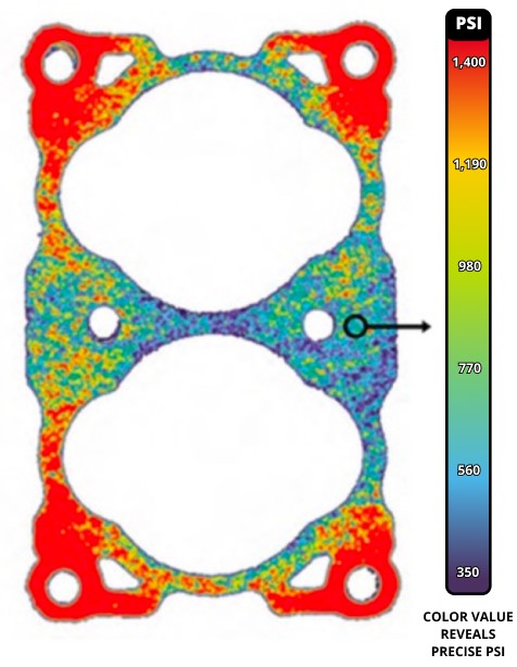
Also, the contact pressure between the substrate and the bottom mold wall could be measured. At this side of the substrate no polymer is injected, but a uniform pressure distribution is important to avoid damage of the solder pads. Figure 5 shows that all solder pads clearly emerge from the flat PCB surface. As the pressure on top of the pads is lowest, the substrate has only mechanical contact to the mold tool with the solder resist, sited between the rectangular pads. The maximum pressure recorded between the mold tool and the PCB substrate is 300 bar, at the edges of the pressure film. The inner area next to the mold cavity shows lower pressure values ~150 to 200 bar. They are corresponding to the pressure applied by the EMC in the cavity (Figure 4). Because the solder pads have no contact to the bottom mold, the pressure at the bearing are is increased.
Conclusions
Pressure measurement films, such as the Pressurex® sensor film used in this study, have been proven to be appropriate sensors to characterize encapsulation of microelectronic systems. The correct characterization of this manufacturing process is essential for all further quality and reliability analyses. The methods and insights presented can be used for the development of stress minimized packaging processes and can be the basis for an enhanced reliability characterization of microelectronic and mechatronic systems regarding polymer encapsulation processes.
![Figure 5: Pressure distribution over the bottom side of the substrate and its bond pad, as imaged [6].](https://www.sensorprod.com/wp-content/uploads/2023/08/substrate.jpg)
Figure 5: Pressure distribution over the bottom
side of the substrate and its bond pad, as imaged [6].
References
- Pressurex Sensor Film, www.sensorprod.com, Sensor Products Inc. (USA).
- R. Müller-Fiedler, V. Knobloch, “Reliability aspects of microsensors and micro-mechatronic actuators for automotive applications,” Microelectronics Reliability 2003; 43: 1085-1091.
- K. Niehoff, T. Schreier-Alt, F. Schindler-Saefkow, F. Ansorge, H. Kittel, “Thermo-Mechanical Stress Analysis,” IEEE European Microelectronics and Packaging Congress EMPC, 2009.
- T. Schreier-Alt, F. Schindler-Saefkow, O. Wittler, H. Kittel, “Encapsulation of system in package – process characterization and optimization,” Proceedings of 2nd ESTC, 2008.
- T. Schreier-Alt, F. Ansorge, H. Reichl, “Fiber Optic Strain and Structural Health Monitoring in Polymer Electronic Packaging,” Proceedings of Electronic Components and Technology Conference, 2007.
- Topaq Analysis System, www.sensorprod.com/topaq, Sensor Products Inc. (USA).
About Fraunhofer IZM – MMZ
Since its establishment in 1993, Fraunhofer IZM (Germany) has become one of the leading research institutions in the field of electronic packaging and system integration worldwide. The company is dedicated to keeping manufacturers and users of microelectronic products on top of technological developments, covering everything from material selection, simulation, design and interconnection technologies up to the transfer into customers’ production line. Micro-Mechatronic Systems, near Munich, develops technologies for mechatronic systems containing mechanical, electrical and software functions. Advanced research is performed with the focus on novel interconnection and encapsulation methods.


